ADM3202/ADM3222/ADM1385
Rev. E | Page 8 of 16
GENERAL DESCRIPTION
The ADM3202/ADM3222/ADM1385 are RS-232 line drivers/
receivers. Step-up voltage converters coupled with level-shifting
transmitters and receivers allow RS-232 levels to be developed
while operating from a single 3.3 V supply.
CMOS technology is used to keep the power dissipation to an
absolute minimum, allowing maximum battery life in portable
applications.
The ADM3202/ADM3222/ADM1385 are modifications,
enhancements, and improvements of the AD230 to AD241
family and derivatives. They are essentially plug-in compatible
and do not have any materially different applications.
CIRCUIT DESCRIPTION
The internal circuitry consists of these main sections:
• A charge pump voltage converter
• 3.3 V logic to EIA-232 transmitters
• EIA-232 to 5 V logic receivers
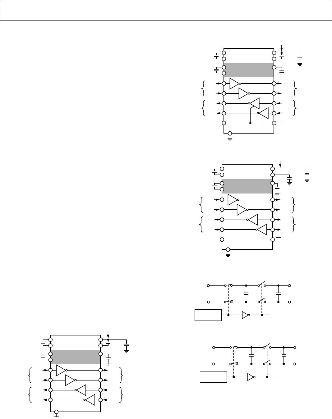
Charge Pump DC to DC Voltage Converter
The charge pump voltage converter consists of a 200 kHz
oscillator and a switching matrix. The converter generates a
±6.6 V supply from the input 3.3 V level. This is done in two
stages by using a switched capacitor technique as illustrated in
Figure 18 and Figure 19. First, the 3.3 V input supply is doubled
to 6.6 V by using Capacitor C1 as the charge storage element.
The +6.6 V level is then inverted to generate −6.6 V using C2
as the storage element. C3 is shown connected between V+ and
V
CC
but is equally effective if connected between V+ and GND.
Capacitors C3 and C4 are used to reduce the output ripple.
Their values are not critical and can be increased, if desired.
Capacitor C3 is shown connected between V+ and V
CC
. It is
also acceptable to connect this capacitor between V+ and GND.
If desired, larger capacitors (up to 10 μF) can be used for
Capacitors C1 to C4.
C1+
C2+
C1–
C2–
V
CC
V–
V+
T1
IN
T1
OUT
T2
IN
T2
OUT
R1
OUT
R1
IN
R2
OUT
R2
IN
CMOS
INPUTS
EIA/TIA-232
OUTPUTS
CMOS
OUTPUTS
EIA/TIA-232
INPUTS*
T1
T2
R1
R2
+
+
+
0.1µF
10V
0.1µF
10V
GND
ADM3202
C3
0.1µF
6.3V
+3.3
INPUT
+3.3V TO +6.6V
VOLTAGE
DOUBLER
+6.6V TO –6.6V
VOLTAGE
INVERTER
C5
0.1µF
+
C4
0.1µF
10V
+
*INTERNAL 5kΩ PULL-DOWN RESISTOR
ON EACH RS-232 INPUT
00071-015
Figure 15. ADM3202 Typical Operating Circuit
C1+
C2+
C1–
C2–
V
CC
V–
V+
T1
IN
T1
OUT
T2
IN
T2
OUT
R1
OUT
R1
IN
R2
OUT
EN
R2
IN
SD
CMOS
INPUTS
EIA/TIA-232
OUTPUTS
CMOS
OUTPUTS
EIA/TIA-232
INPUTS*
T1
T2
R1
R2
+
+
+
0.1µF
10V
0.1µF
10V
GND
ADM3222
C3
0.1µF
6.3V
+3.3
INPUT
+3.3V TO +6.6V
VOLTAGE
DOUBLER
+6.6V TO –6.6V
VOLTAGE
INVERTER
C5
0.1µF
+
C4
0.1µF
10V
+
*INTERNAL 5kΩ PULL-DOWN RESISTOR
ON EACH RS-232 INPUT
00071-016
Figure 16. ADM3222 Typical Operating Circuit
C1+
C2+
C1–
C2–
V
CC
V–
V+
T1
IN
T1
OUT
T2
IN
T2
OUT
R1
OUT
R1
IN
R2
OUT
DD
R2
IN
SD
CMOS
INPUTS
EIA/TIA-232
OUTPUTS
CMOS
OUTPUTS
EIA/TIA-232
INPUTS*
T1
T2
R1
R2
+
+
0.1µF
10V
0.1µF
10V
GND
ADM1385
+3.3V INPUT
+3.3V TO +6.6V
VOLTAGE
DOUBLER
+6.6V TO –6.6V
VOLTAGE
INVERTER
C5
0.1µF
+
+
+
*INTERNAL 5kΩ PULL-DOWN RESISTOR
ON EACH RS-232 INPUT
00071-017
C3
0.1µF
10V
C4
0.1µF
10V
Figure 17. ADM1385 Typical Operating Circuit
C1
+
C3
+
S3
S4
S1
S2
INTERNAL
OSCILLATOR
V
CC
GND
V
CC
V+ = 2V
CC
00071-018
Figure 18. Charge Pump Voltage Doubler
C2
+
C4
+
S3
S4
S1
S2
INTERNAL
OSCILLATOR
V
+
GND
V– = –(V+)
GND
FROM
VOLTAGE
DOUBLER
00071-019
Figure 19. Charge Pump Voltage Inverter

