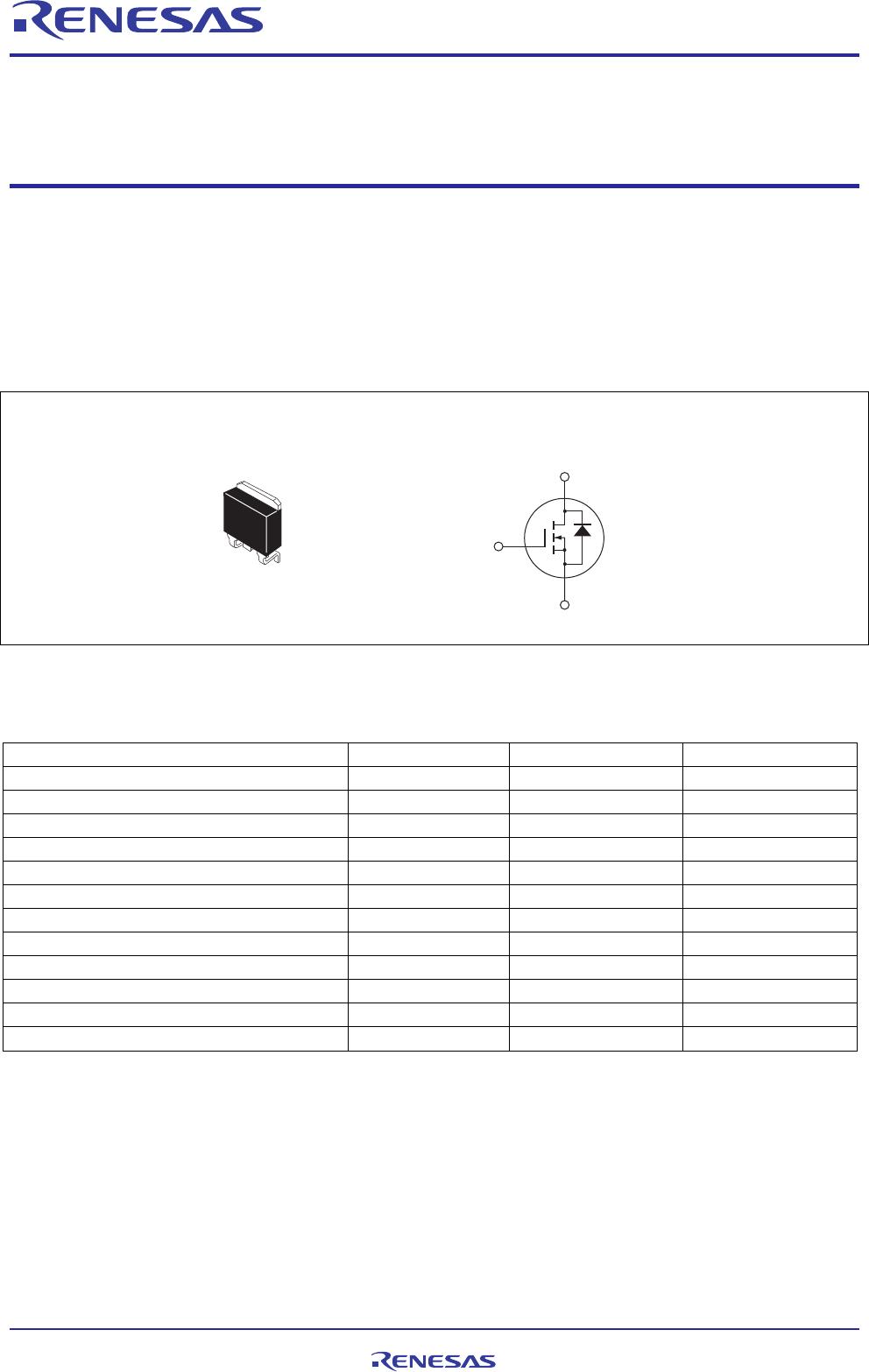
RJK6013DPE Preliminary
R07DS0486EJ0200 Rev.2.00 Page 2 of 6
Jun 21, 2012
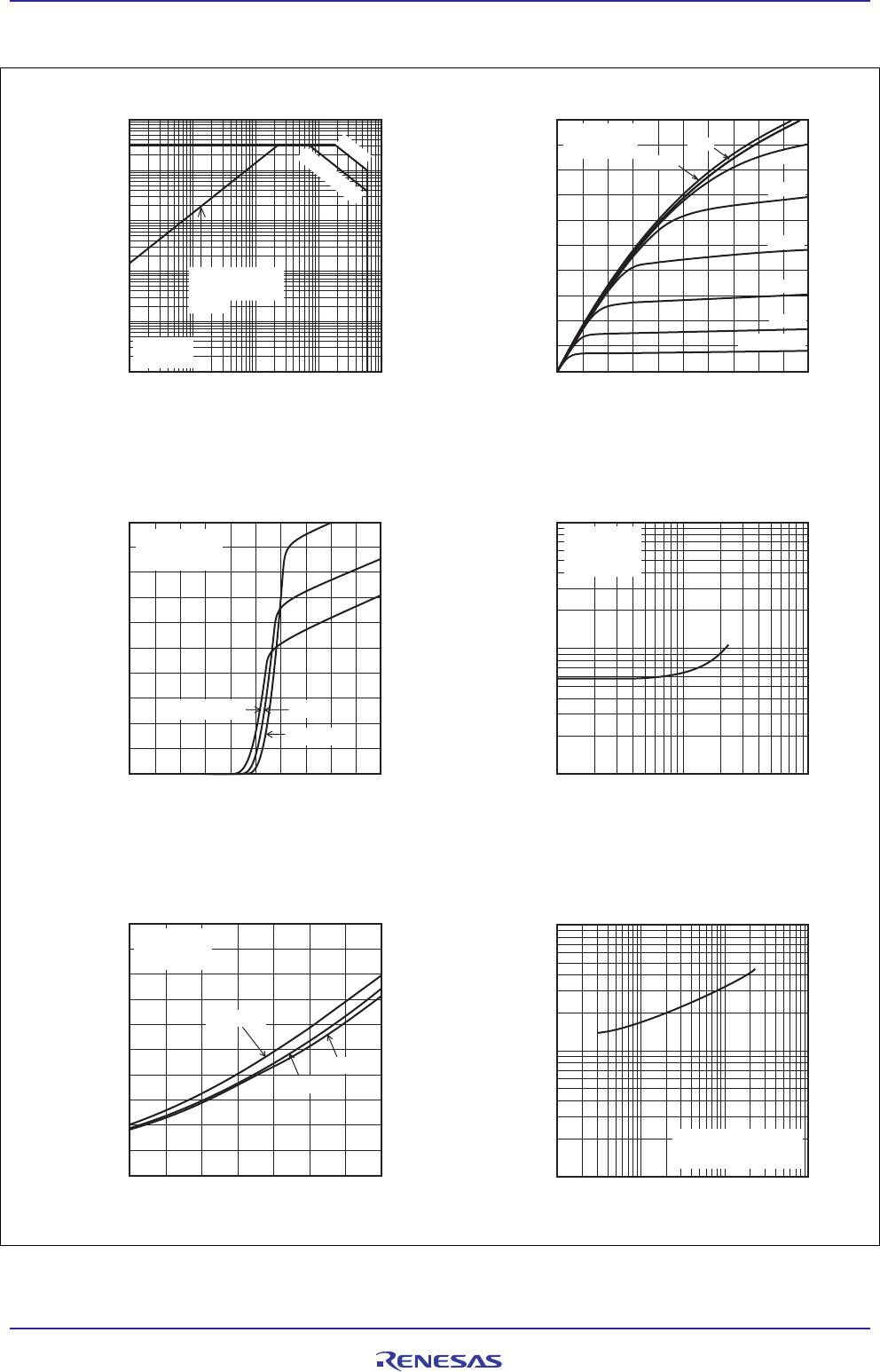
Electrical Characteristics
(Ta = 25°C)
Item Symbol Min Typ Max Unit Test conditions
Drain to source breakdown voltage V
(BR)DSS
600 — — V I
D
= 10 mA, V
GS
= 0
Zero gate voltage drain current I
DSS
— — 1 A V
DS
= 600 V, V
GS
= 0
Gate to source leak current I
GSS
— — 0.1 A V
GS
= 30 V, V
DS
= 0
Gate to source cutoff voltage V
GS(off)
3.0 — 4.5 V V
DS
= 10 V, I
D
= 1 mA
Static drain to source on state
resistance
R
DS(on)
— 0.58 0.70 I
D
= 5.5 A, V
GS
= 10 V
Note4
Input capacitance Ciss — 1450 — pF
Output capacitance Coss — 140 — pF
Reverse transfer capacitance Crss — 17 — pF
V
DS
= 25 V
V
GS
= 0
f = 1 MHz
Turn-on delay time t
d(on)
— 33 — ns
Rise time t
r
— 20 — ns
Turn-off delay time t
d(off)
— 87 — ns
Fall time t
f
— 15 — ns
I
D
= 5.5 A
V
GS
= 10 V
R
L
= 54.5
Rg = 10
Total gate charge Qg — 37.5 — nC
Gate to source charge Qgs — 7.3 — nC
Gate to drain charge Qgd — 16.4 — nC
V
DD
= 480 V
V
GS
= 10 V
I
D
= 11 A
Body-drain diode forward voltage V
DF
— 0.87 1.45 V I
F
= 11 A, V
GS
= 0
Note4
Body-drain diode reverse recovery time t
rr
— 350 — ns
I
F
= 11 A, V
GS
= 0
di
F
/dt = 100 A/s
Notes: 4. Pulse test