BS870-7-F

BS870
Document number: DS11302 Rev. 18 - 2
1 of 5
www.diodes.com
August 2013
© Diodes Incorporated
BS870
N-CHANNEL ENHANCEMENT MODE MOSFET
Features
Low On-Resistance
Low Gate Threshold Voltage
Low Input Capacitance
Fast Switching Speed
Low Input/Output Leakage
Totally Lead-Free & Fully RoHS Compliant (Notes 1 & 2)
Halogen and Antimony Free. “Green” Device (Notes 3 & 4)
Qualified to AEC-Q101 Standards for High Reliability
Mechanical Data
Case: SOT23
Case Material: Molded Plastic. UL Flammability Classification
Rating 94V-0
Moisture Sensitivity: Level 1 per J-STD-020
Terminal Connections: See Diagram
Terminals: Matte Tin Finish annealed over Alloy 42 leadframe
(Lead Free Plating). Solderable per MIL-STD-202, Method 208
Weight: 0.008 grams (approximate)
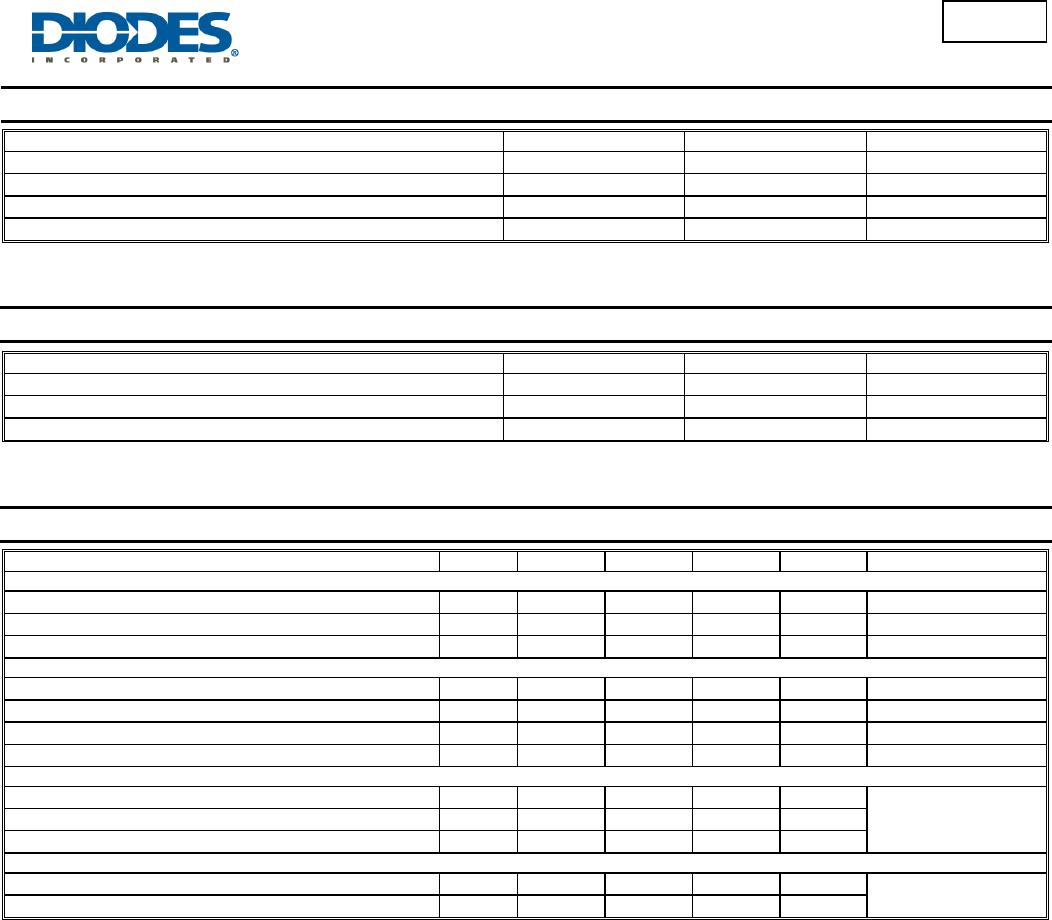
Ordering Information (Note 5)
Part Number Case Packaging
BS870-7-F SOT23 3000/Tape & Reel
Notes: 1. No purposely added lead. Fully EU Directive 2002/95/EC (RoHS) & 2011/65/EU (RoHS 2) compliant.
2. See http://www.diodes.com/quality/lead_free.html for more information about Diodes Incorporated’s definitions of Halogen- and Antimony-free, "Green"
and Lead-free.
3. Halogen- and Antimony-free "Green” products are defined as those which contain <900ppm bromine, <900ppm chlorine (<1500ppm total Br + Cl) and
<1000ppm antimony compounds.
4. Product manufactured with Date Code V9 (week 33, 2008) and newer are built with Green Molding Compound. Product manufactured prior to Date
Code V9 are built with Non-Green Molding Compound and may contain Halogens or Sb
2
O
3
Fire Retardants.
5. For packaging details, go to our website at http://www.diodes.com/products/packages.html
Marking Information
Date Code Key
Year 1998 1999 2000 2001 2002 2003 2004 2011 2012 2013 2014 2015 2016 2017
Code J K L M N P R Y Z A B C D E
Month Jan Feb Mar Apr May Jun Jul Aug Sep Oct Nov Dec
Code 1 2 3 4 5 6 7 8 9 O N D
SOT23
Top View Equivalent Circuit
To
p
View
K70 = Product Type Marking Code
YM = Date Code Marking for SAT (Shanghai Assembly/ Test site)
= Date Code Marking for CAT (Chengdu Assembly/ Test site)
Y or = Year (ex: A = 2013)
M = Month (ex: 9 = September)
D
G
S
Source
Gate
Drain
Shanghai A/T SiteChengdu A/T Site
Y
M
Y
K70
YM
K70
YM
BS870
Document number: DS11302 Rev. 18 - 2
2 of 5
www.diodes.com
August 2013
© Diodes Incorporated
BS870
Maximum Ratings (@T
A
= +25°C, unless otherwise specified.)
Characteristic Symbol Value Units
Drain-Source Voltage
V
DSS
60 V
Drain-Gate Voltage R
GS
1.0M V
DGR
60 V
Gate-Source Voltage Continuous
V
GSS
20
V
Drain Current (Note 6) Continuous
I
D
250 mA
Thermal Characteristics (@T
A
= +25°C, unless otherwise specified.)
Characteristic Symbol Value Units
Total Power Dissipation (Note 6)
P
D
300 mW
Thermal Resistance, Junction to Ambient
R
JA
417
C/W
Operating and Storage Temperature Range
T
J
, T
STG
-55 to +150
C
Electrical Characteristics (@T
A
= +25°C, unless otherwise specified.)
Characteristic Symbol Min Typ Max Unit Test Condition
OFF CHARACTERISTICS (Note 7)
Drain-Source Breakdown Voltage
BV
DSS
60 80
V
V
GS
= 0V, I
D
= 100A
Zero Gate Voltage Drain Current
I
DSS
0.5 µA
V
DS
= 25V, V
GS
= 0V
Gate-Body Leakage
I
GSS
10
nA
V
GS
= 15V, V
DS
= 0V
ON CHARACTERISTICS (Note 7)
Gate Threshold Voltage
V
GS
(
th
)
1.0 2.0 3.0 V
V
DS
= V
GS
, I
D
= 250A
Static Drain-Source On-Resistance
R
DS
(
ON
)
3.5 5.0
V
GS
= 10V, I
D
= 0.2A
On-State Drain Current
I
D
(
ON
)
0.5 1.0
A
V
GS
= 10V, V
DS
= 7.5V
Forward Transconductance
g
FS
80
mS
V
DS
=10V, I
D
= 0.2A
DYNAMIC CHARACTERISTICS
Input Capacitance
C
iss
22 50 pF
V
DS
= 10V, V
GS
= 0V
f = 1.0MHz
Output Capacitance
C
oss
11 25 pF
Reverse Transfer Capacitance
C
rss
2.0 5.0 pF
SWITCHING CHARACTERISTICS
Turn-On Delay Time
t
D
(
ON
)
2.0 20 ns
V
ES
= 10V, R
L
= 150,
V
DS
= 10V, R
D
= 100 Turn-Off Delay Time
t
D
(
OFF
)
5.0 20 ns
Notes: 6. Device mounted on FR-4 PCB 1.0 x 0.75 x 0.062 inch pad layout as shown on Diodes, Inc. suggested pad layout AP02001, which can be found on
our website at http://www.diodes.com.
7. Short duration pulse test used to minimize self-heating effect.
BS870
Document number: DS11302 Rev. 18 - 2
3 of 5
www.diodes.com
August 2013
© Diodes Incorporated
BS870
0
0.2
0.4
0.6
0.8
1.0
01
2
3
45
V , DRAIN-SOURCE VOLTAGE (V)
Fig. 1 On-Region Characteristics
DS
I DRAIN-SOURCE CURRENT (A)
D
,
0
1
2
3
4
5
00.2
, N
MALIZED
DRAIN-SOURCE ON-RESISTANCE
DS(ON)
I , DRAIN CURRENT (A)
Fig. 2 On-Resistance vs. Drain Current
D
6
7
0.4 0.6 0.8 1.0
0
0.5
1.0
1.5
2.0
-55 -30 -5 20 45
70
95 120 145
, N
MALIZED
DRAIN-SOURCE ON-RESISTANCE
DS(ON)
T, JUNCTION TEMPERATURE ( C)
Fig. 3 On-Resistance vs. Junction Temperature
j
°
0
V , GATE TO SOURCE VOLTAGE (V)
Fig. 4 On-Resistance vs. Gate-Source Voltage
GS
1
2
3
4
5
6
0 2 4 6 8 1012141618
R , NORMALIZED
DRAIN-SOURCE ON-RESISTANCE
DS(ON)
0
50
100
25 50
75
100 125
150 175 200
,
WE
DISSI
A
I
N (mW)
D
T , AMBIENT TEMPERATURE (°C)
Fig. 5 Max Power Dissipation vs. Ambient Temperature
A
150
200
250
300
350
0
400

BS870-7-F

Mfr. #:
Manufacturer:
Diodes Incorporated
Description:
MOSFET 60V 310mW
Lifecycle:
New from this manufacturer.
Delivery:
DHL FedEx Ups TNT EMS
Payment:
T/T Paypal Visa MoneyGram Western Union

Products related to this Datasheet