AD830
Rev. C | Page 12 of 20
V
X1
V
OUT
I
Y
I
X
C
C
A = 1
G
M
A
OLS
=
G
M
R
P
V
X2
G
M
V
Y1
V
Y2
R
P
I
Z
I
X
= (V
X1
– V
X2
) G
M
I
Y
= (V
Y1
– V
Y2
) G
M
I
Z
= I
X
+ I
Y
1 + S (C
C
R
P
)
0
0881-026
Figure 26. Topology Diagram
V
X1
V
OUT
I
Y
I
X
C
C
A = 1
G
M
1
V
X2
G
M
V
Y1
V
Y2
V
X1
– V
X2
= V
Y2
– V
Y1
FOR V
Y2
= V
OUT
V
OUT
= (V
X1
– V
X2
+ V
Y1
)
1 + S(C
C
/G
M
)
00881-027
Figure 27. Closed-Loop Connection
Precise amplification is accomplished through closed-loop
operation of this topology. Voltage feedback is implemented via
the Y G
M
stage where the output is connected to the −Y input
for negative feedback, as shown in Figure 27. An input signal is
applied across the X G
M
stage, either fully differential or single-
ended referred to common. It produces a current signal that is
summed at the high impedance node with the output current
from the Y G
M
stage. Negative feedback nulls this sum to a small
error current necessary to develop the output voltage at the high
impedance node. The error current is usually negligible, so the
null condition essentially forces the Y G
M
output stage current
to equal the exact X G
M
output current. Because the two
transconductances are identical, the differential voltage across
the Y inputs equals the negative of the differential voltage across
the X input; V
Y
= −V
X
or, more precisely, V
Y2
− V
Y1
= V
X1
− V
X2
.
This simple relation provides the basis to easily analyze any
function possible to synthesize with the AD830, including any
feedback situation.
The bandwidth of the circuit is defined by the G
M
and the
capacitor, C
C
. The highly linear G
M
stages give the amplifier a
single-pole response, excluding the output amplifier and
loading effects. It is important to note that the bandwidth and
general dynamic behavior is symmetrical (identical) for the
noninverting and the inverting connections of the AD830. In
addition, the input impedance and CMRR are the same for
either connection. This is very advantageous and unlike in a
voltage or current feedback amplifier where there is a distinct
difference in performance between the inverting and
noninverting gain. The practical importance of this cannot be
overemphasized and is a key feature offered by the AD830
amplifier topology.
INTERFACING THE INPUT
Common-Mode Voltage Range
The common-mode range of the AD830 is defined by the
amplitude of the differential input signal and the supply voltage.
The general definition of common-mode voltage, V
CM
, is
usually applied to a symmetrical differential signal centered
around a particular voltage, as illustrated in Figure 28. This is
the meaning implied here for common-mode voltage. The
internal circuitry establishes the maximum allowable voltage on
the input or feedback pins for a given supply voltage. This
constraint and the differential input voltage sets the common-
mode voltage limit. Figure 29 shows a curve of the common-
mode voltage range versus the differential voltage for three
supply voltage settings.
V
MAX
V
CM
V
PEAK
00881-028
Figure 28. Common-Mode Definition
DIFFERENTIAL INPUTVOLTAGE (V
PEAK
)
15
0
0
COMMON-MODE VOLT
2.0
A
GE (±V)
0.4 0.8 1.2 1.6
6
3
12
9
±5V = V
S
±15V = V
S
–V
CM
–V
CM
+V
CM
+V
CM
+V
CM
±10V = V
S
–V
CM
00881-029
Figure 29. Input Common-Mode Voltage Range vs. Differential Input Voltage
Differential Voltage Range
The maximum applied differential voltage is limited by the
clipping range of the input stages. This is nominally set at a
2.4 V magnitude and depicted in the cross plot (X-Y) in Figure 30.
The useful linear range of the input stages is set at 2 V but is
actually a function of the distortion required for a particular
application. The distortion increases for larger differential input
voltages. A plot of relative distortion versus the input differential
voltage is shown in Figure 13 and Figure 16. The distortion
characteristics impose a secondary limit to the differential input
voltage for high accuracy applications.
AD830
Rev. C | Page 13 of 20
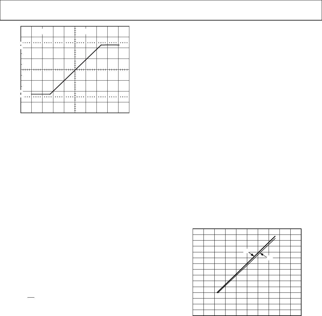
10
0%
100
90
1V 1V
00881-030
Figure 30. Clipping Behavior
Choice of Polarity
The sign of the gain is easily selected by choosing the polarity
of the connections to the + and − inputs of the X G
M
stage.
Swapping between inverting and noninverting gain is possible
simply by reversing the input connections. The response of the
amplifier is identical in either connection, except for the sign
change.
The bandwidth, high impedance, and transient behavior of the
AD830 is symmetrical for both polarities of gain. This is very
advantageous and unlike an op amp.
Input Impedance
The relatively high input impedance of the AD830, for a
differential receiver amplifier, permits connections to modest
impedance sources without much loading or loss of common-
mode rejection. The nominal input resistance is 300 k. The
real limit to the upper value of the source resistance is in its
effect on common-mode rejection and bandwidth. If the source
resistance is in only one input, then the low frequency
common-mode rejection is lowered to ≈ R
IN
/R
S
. The source
resistance/input capacitance pole limits the bandwidth. Refer to
the following equation:
××
π
=
IN
S
CRf
2
1
Furthermore, the high frequency common-mode rejection is
additionally lowered by the difference in the frequency response
caused by the R
S
× C
IN
pole. Therefore, to maintain good low
and high frequency common-mode rejection, it is recommended
that the source resistances of the + and − inputs be matched and
of modest value (≤10 k).
Handling Bias Currents
The bias currents are typically 4 A flowing into each pin of the
G
M
stages of the AD830. Because all applications possess some
finite source resistance, the bias current through this resistor
creates a voltage drop (I
BIAS
× R
S
). The relatively high input
impedance of the AD830 permits modest values of R
S
, typically
≤10 k. If the source resistance is in only one terminal, then an
objectionable offset voltage may result, for example, 4 A × 5
k = 20 mV. Placement of an equal value resistor in series with
mismatches in the resistances, a residual offset remains and is
likely to be greater than the bias current (offset current)
mismatches.
Applying Fee
the other input cancels the offset to first order. However, due to
dback
for use with gains from 1 to 100. Gains
hat
y
830 is defined by the differential
n
ge
e
The AD830 is intended
greater than one are simply set by a pair of resistors connected
as shown in the difference amplifier (Figure 40) with gain >1.
The value of the bottom resistor, R
2
, should be kept less than
1 k to ensure that the pole formed by C
IN
and the parallel
connection of R
1
and R
2
is sufficiently high in frequency so t
it does not introduce excessive phase shift around the loop and
destabilize the amplifier. A compensating resistor, equal to the
parallel combination of R
1
and R
2
, should be placed in series
with the other Y G
M
stage input to preserve the high frequenc
common-mode rejection and to lower the offset voltage
induced by the input bias current.
Output Common Mode
The output swing of the AD
input voltage, the gain, and the output common. Depending o
the anticipated signal span, the output common (or ground)
may be set anywhere between the allowable peak output volta
in a manner similar to that described for input voltage common
mode. A plot of the peak output voltage versus the supply is
shown in Figure 31. A prediction of the common-mode rang
versus the peak output differential voltage can be easily derived
from the maximum output swing as V
OCM
= V
MAX
− V
PEAK
.
SUPPLY VOLTAGE (V)
15
0
200
MAXIMUM OUTPUT SWING (±V)
481216
6
3
12
9
V
P
V
N
00881-031
Figure 31. Maximum Output Swing vs. Supply
Output Cur
output current is set by the short-circuit
nto
rent
The absolute peak
current limiting, typically greater than 60 mA. The maximum
drive capability is rated at 50 mA but without a guarantee of
distortion performance. Best distortion performance is obtained
by keeping the output current ≤20 mA. Attempting to drive
large voltages into low valued resistances, for example, 10 V i
150  causes an apparent lowering of the limit for output signal
swing but is just the current limiting behavior.
AD830
Rev. C | Page 14 of 20
Driving Cap Loads
The AD830 is capable of driving modest sized capacitive loads
while maintaining its rated performance. Several curves of
bandwidth versus capacitive load are given in Figure 34 and
Figure 37. The AD830 was designed primarily as a low
distortion video speed amplifier but with a trade-off, for
example, giving up very large capacitive load driving capability.
If very large capacitive loads must be driven, the network shown
in Figure 32 should be used to ensure stable operation. If the
loss of gain caused by the resistor, R
S
, in series with the load is
objectionable, the optional feedback network shown may be
added to restore the lost gain.
+
V
S
V
OUT
R
S
36.5
*OPTIONAL
FEEDBACK
NETWORK
–V
S
AD830
1
2
3
4
8
7
6
5
A = 1
G
M
G
M
C
0.1µF
0.1µF
C
1
100pF
R
S
R
2
R
1
1k
INPUT
SIGNAL
V
CM
Z
CM
00881-032
Figure 32. Circuit for Driving Large Capacitive Loads
FREQUENCY (Hz)
3
10k
CLOSED-LOOP AMPLITUDE RESPONSE (dB)
–27
100k 1M 10M
100M
±15V
±5V
–24
–21
–18
–15
–12
–9
–6
–3
0
00881-033
Figure 33. Closed-Loop Response vs. Frequency with 100 pF Load and Series
Resistor Compensation
SUPPLIES, BYPASSING, AND GROUNDING
(FIGURE 34)
The AD830 is capable of operating over a wide range of supply
voltages, both single and dual supplies. The coupling may be dc
or ac, provided the input and output voltages stay within the
specified common-mode voltage limits. For dual supplies, the
device works from ±4 V to ±16.5 V. Single-supply operation is
possible over 8 V to 33 V. It is also possible to operate the part
with split-supply voltages, for example, +24 V or −5 V for
special applications such as level shifting. The primary
constraint is that the total potential between the two supplies
does not exceed 33 V.
Inclusion of power supply bypassing capacitors is necessary to
achieve stable behavior and the specified performance. It is
especially important when driving low resistance loads. At
minimum, connect a 0.1 F ceramic capacitor at the supply lead
of the AD830 package. In addition, for the best bypassing, it is
best to connect a 0.01 F ceramic capacitor and 4.7 F tantalum
capacitor to the supply lead going to the AD830.
0.1µF
0.01µF
V
P
AND
V
N
V
P
AND
V
N
4.7µF
LOAD
GND
LEAD
LOAD
GND
LEAD
0
0881-034
Figure 34. Supply Decoupling Options
The AD830 is designed to be capable of rejecting noise and
dissimilar potentials in the ground lines. Therefore, proper
care is necessary to realize the benefits of the differential
amplification of the part. Separation of the input and output
grounds is crucial in rejection of the common-mode noise at
the inputs and eliminating any ground drops on the input signal
line. For example, connecting the ground of a coaxial cable to
the AD830 output common (board ground) could degrade the
CMR and also introduce power-down loading on cable grounds.
However, it is also necessary as in any electronic system to
provide a return path for bias currents back to their original
power supply. This is accomplished by providing a connection
between the differing grounds through a modest impedance
labeled Z
CM
, for example, 100 .
Single-Supply Operation
The AD830 is capable of operating in single power supply
applications down to a voltage of 8 V, with the generalized
connection shown in Figure 35. There is a constraint on the
common-mode voltage at the input and output that establishes
the range for these voltages. Direct coupling may be used for
input and output voltages that lie in these ranges. Any gain
network applied needs to be referred to the output common
connection or have an appropriate offset voltage. In situations
where the signal lies at a common voltage outside the common-
mode range of the AD830, direct coupling does not work, so ac
coupling should be used. Figure 47 shows how to easily
accomplish coupling to the AD830. For single-supply operation
where direct coupling is desired, the input and output common-
mode curves (Figure 36 and Figure 37) should be used.

AD830JR-REEL

Mfr. #:
Manufacturer:
Analog Devices Inc.
Description:
Differential Amplifiers HI SPEED VIDEO
Lifecycle:
New from this manufacturer.
Delivery:
DHL FedEx Ups TNT EMS
Payment:
T/T Paypal Visa MoneyGram Western Union