32MB, 64MB, 128MB (x72, SR)
168-PIN SDRAM UDIMM
32, 64, 128MB x 64 SDRAM DIMM Micron Technology, Inc., reserves the right to change products or specifications without notice.
SD5C4_8_16x72AG.fm - Rev. C 6/04 EN
4 ©2004 Micron Technology, Inc. All rights reserved.
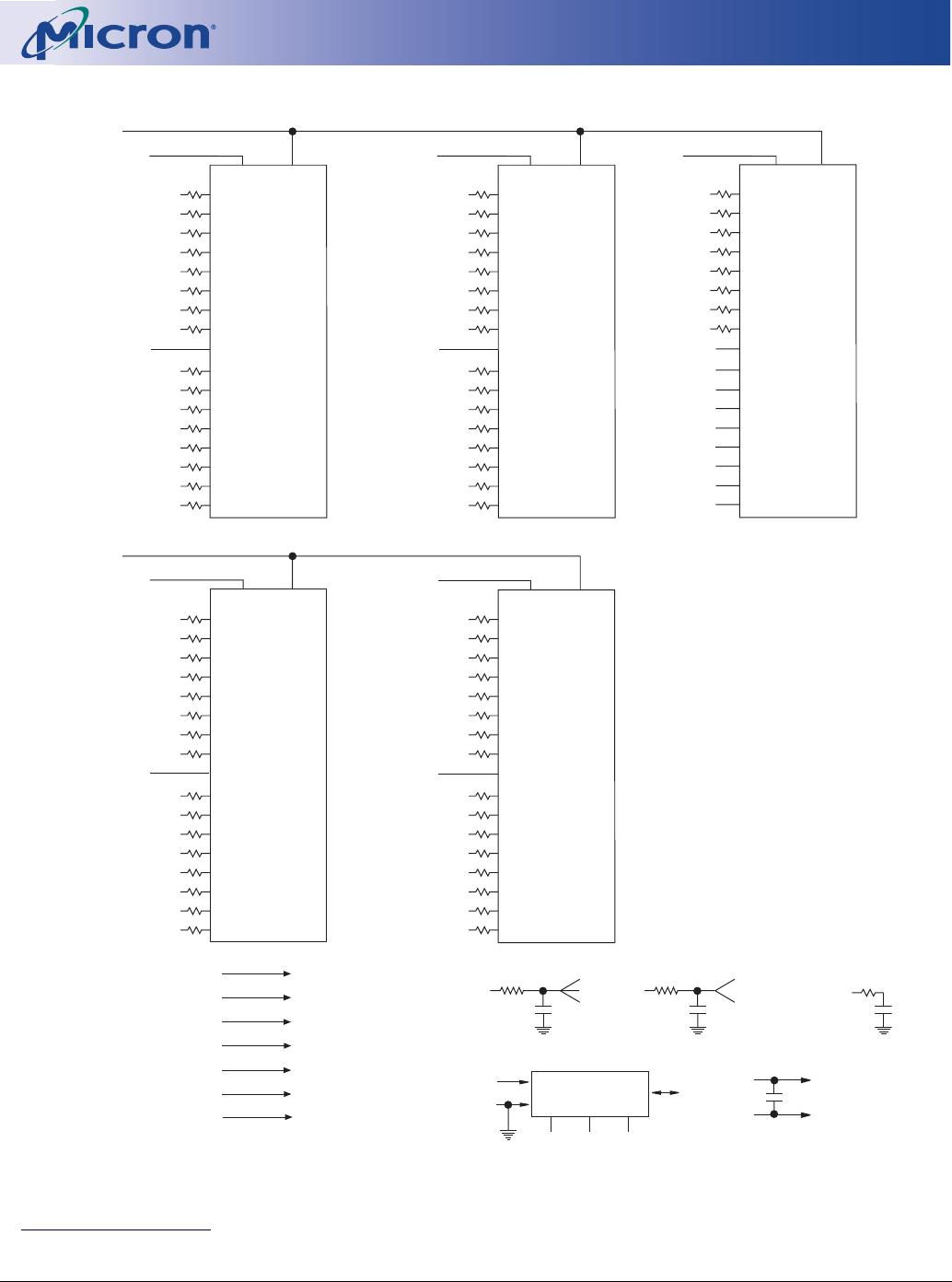
Table 6: PIN Descriptions
Pins may not correlate with symbols; refer to Pin Assignment tables on page 3 for more information
PIN NUMBERS SYMBOL TYPE DESCRIPTION
27, 111, 115 RAS#, CAS#, WE#, Input
Command Inputs: RAS#, CAS#, and WE# (along with S#) define
the command being entered.
42, 79 CK0, CK2 Input
Clock: CK is driven by the system clock. All SDRAM input
signals are sampled on the positive edge of CK. CK also
increments the internal burst counter and controls the output
registers.
128 CKE0 Input
Clock Enable: CKE activates (HIGH) and deactivates (LOW) the
CK signal. Deactivating the clock provides PRECHARGE
POWER-DOWN and SELF REFRESH operation (all device banks
idle) or CLOCK SUSPEND OPERATION (burst access in progress).
CKE is synchronous except after the device enters power-down
and self refresh modes, where CKE becomes asynchronous
until after exiting the same mode. The input buffers, including
CK, are disabled during power-down and self refresh modes,
providing low standby power.
30, 45 S0#, S2# Input
Chip Select: S# enables (registered LOW) and disables
(registered HIGH) the command decoder. All commands are
masked when S# is registered HIGH. S# is considered part of
the command code.
28, 29, 46, 47, 112, 113,
130, 131
DQMB0–DQMB7 Input
Input/Output Mask: DQMB is an input mask signal for write
accesses and an output enable signal for read accesses. Input
data is masked when DQMB is sampled HIGH during a WRITE
cycle. The output buffers are placed in a High-Z state (two-
clock latency) when DQMB is sampled HIGH during a READ
cycle.
39, 122 BA0, BA1 Input
Bank Address: BA0 and BA1 define to which device bank the
ACTIVE, READ, WRITE, or PRECHARGE command is being
applied.
33–38, 117–121, 123,
126 (128MB)
A0–A11
(32MB/64MB)
A0–A12
(128MB)
Input
Address Inputs: Provide the row address for ACTIVE
commands, and the column address and auto prcharge bit
(A10) for READ/WRITE commands, to select one location out of
the memory arrary in the respective device bank. A10 sampled
during a PRECHARGE command determines whether the
PRECHARGE applies to one device bank (A10 LOW – device
bank selected by BA0, BA1) or all device banks (A10 HIGH). The
address inputs also provide the op-code during a MODE
REGISTER SET command.
83 SCL Input
Serial Clock for Presence-Detect: SCL is used to synchronize the
presence-detect data transfer to and from the module.
165-167 SA0–SA2 Input
Presence-Detect Address Inputs: These pins are used to
configure the presence-detect device.
82 SDA Input/Output
Serial Presence-Detect Data: SDA is a bidirectional pin used to
transfer addresses and data into and out of the presence-
detect portion of the module.
2–5, 7–11, 13–17, 19–20,
55–58, 60, 65–67, 69–72,
74–77, 86–89, 91–95, 97–
101, 103–104, 139–142,
144, 149–151, 153–156,
158–161
DQ0–DQ63 Input/Output
Data I/Os: Data bus.