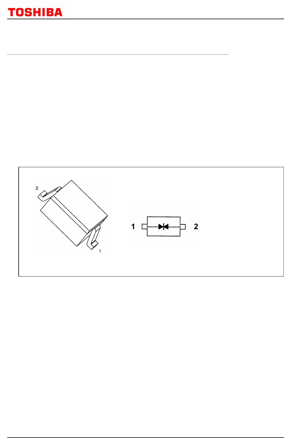
DF2B18FU,H3F

DF2B18FU
1
ESD Protection Diodes Silicon Epitaxial Planar
DF2B18FU
DF2B18FU
DF2B18FU
DF2B18FU
Start of commercial production
2015-05
1.
1.
1.
1. Applications
Applications
Applications
Applications
ESD Protection
Note: This product is designed for protection against electrostatic discharge (ESD) and is not intended for any other
purpose, including, but not limited to, voltage regulation.
2.
2.
2.
2. Features
Features
Features
Features
(1) AEC-Q101 qualified (Note 1)
Note 1: For detail information, please contact to our sales.
3.
3.
3.
3. Packaging and Internal Circuit
Packaging and Internal Circuit
USC
1: Pin 1
2: Pin 2
2015-05-13
Rev.1.0
DF2B18FU
2
4.
4.
4.
4. Absolute Maximum Ratings (Note) (Unless otherwise specified, T
Absolute Maximum Ratings (Note) (Unless otherwise specified, T
a
a
a
a
= 25
= 25
= 25
= 25
)
)
)
)
Characteristics
Electrostatic discharge voltage (IEC61000-4-2)(Contact)
Electrostatic discharge voltage(IEC61000-4-2)(Air)
Electrostatic discharge voltage(ISO10605)(Contact)
Electrostatic discharge voltage(ISO10605)(Air)
Peak pulse power
Peak pulse current
Junction temperature
Storage temperature
Symbol
V
ESD
V
ESD
P
PK
I
PP
T
j
T
stg
Note
(Note 1)
(Note 2)
(Note 3)
Rating
±30
±30
80
2.5
150
-55 to 150
Unit
kV
kV
W
A
Note: Using continuously under heavy loads (e.g. the application of high temperature/current/voltage and the
significant change in temperature, etc.) may cause this product to decrease in the reliability significantly even
if the operating conditions (i.e. operating temperature/current/voltage, etc.) are within the absolute maximum
ratings.
Please design the appropriate reliability upon reviewing the Toshiba Semiconductor Reliability Handbook
("Handling Precautions"/"Derating Concept and Methods") and individual reliability data (i.e. reliability test
report and estimated failure rate, etc).
Note 1: According to IEC61000-4-2.
Note 2: According to ISO10605. (@ C = 330 pF, R = 2 k)
Note 3: According to IEC61000-4-5.
2015-05-13
Rev.1.0
DF2B18FU
3
5.
5.
5.
5. Electrical Characteristics (Unless otherwise specified, T
Electrical Characteristics (Unless otherwise specified, T
a
a
a
a
= 25
= 25
= 25
= 25
)
)
)
)
V
RWM
: Working peak reverse
voltage
V
BR
: Reverse breakdown voltage
I
BR
: Reverse breakdown current
I
R
: Reverse current
V
C
: Clamp voltage
I
PP
: Peak pulse current
R
DYN
: Dynamic resistance
Fig.
Fig.
Fig.
Fig. 5.1
5.1
5.1
5.1 Definitions of Electrical Characteristics
Definitions of Electrical Characteristics
Characteristics
Reverse breakdown voltage
Reverse current
Clamp voltage
Dynamic resistance
Total capacitance
Symbol
V
BR
I
R
V
C
R
DYN
C
t
Note
(Note 1), (Note 3)
(Note 2)
Test Condition
I
BR
= 1 mA
V
RWM
= 12 V
I
PP
= 1 A
I
PP
= 2.5 A
V
R
= 0 V, f = 1 MHz
Min
16.2
Typ.
19
23
0.8
9
Max
20.5
0.1
33
10
Unit
V
µA
V
V
pF
Note 1: Based on IEC61000-4-5 8/20 µs pulse.
Note 2: TLP parameter: Z0 = 50 , tp = 100 ns, tr = 300 ps, averaging window: t1 = 30 ns to t2 = 60 ns,
extraction of dynamic resistance using a least-squares fit of TLP characteristics at I
PP
between 8 A to 16 A.
Note 3: Guaranteed by design.
2015-05-13
Rev.1.0

DF2B18FU,H3F

Mfr. #:
Manufacturer:
Toshiba
Description:
TVS Diodes / ESD Suppressors ESD Protection Diode SNG Bi-directional
Lifecycle:
New from this manufacturer.
Delivery:
DHL FedEx Ups TNT EMS
Payment:
T/T Paypal Visa MoneyGram Western Union

Products related to this Datasheet