MAX1060/MAX1064
only 50µs are required after power-up. Enter standby
mode by performing a dummy conversion with the con-
trol byte specifying standby mode.
Note: Bypass capacitors larger than 4.7µF between
REF and GND result in longer power-up delays.
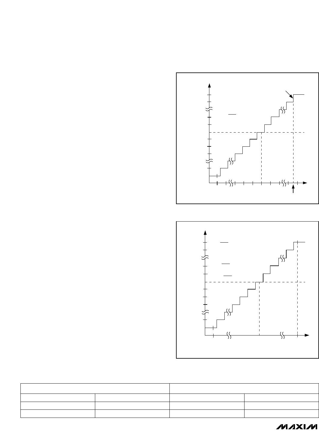
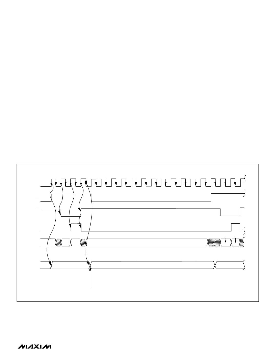
Transfer Function
Table 6 shows the full-scale voltage ranges for unipolar
and bipolar modes.
Figure 8 depicts the nominal, unipolar input/output (I/O)
transfer function, and Figure 9 shows the bipolar I/O
transfer function. Code transitions occur halfway
between successive-integer LSB values. Output coding
is binary, with 1 LSB = V
REF
/ 1024.
Maximum Sampling Rate/
Achieving 475ksps
When running at the maximum clock frequency of
7.6MHz, the specified 400ksps throughput is achieved
by completing a conversion every 19 clock cycles: 1
write cycle, 3 acquisition cycles, 13 conversion cycles,
and 2 read cycles. This assumes that the results of the
last conversion are read before the next control byte is
written. It is possible to achieve higher throughputs
(Figure 10), up to 475ksps, by first writing a control
word to begin the acquisition cycle of the next conver-
sion, then reading the results of the previous conver-
sion from the bus. This technique allows a conversion
to be completed every 16 clock cycles. Note that
switching the data bus during acquisition or conversion
can cause additional supply noise that can make it diffi-
cult to achieve true 10-bit performance.
Layout, Grounding, and Bypassing
For best performance, use printed circuit boards. Wire-
wrap configurations are not recommended since the lay-
out should ensure proper separation of analog and digital
traces. Do not run analog and digital lines parallel to each
other, and do not lay out digital signal paths underneath
the ADC package. Use separate analog and digital PC
board ground sections with only one star point (Figure
11) connecting the two ground systems (analog and digi-
tal). For lowest noise operation, ensure the ground return
to the star ground’s power supply is low impedance and
as short as possible. Route digital signals far away from
sensitive analog and reference inputs.
400ksps, +5V, 8-/4-Channel, 10-Bit ADCs
with +2.5V Reference and Parallel Interface
16 ______________________________________________________________________________________
111 . . . 111
111 . . . 110
100 . . . 010
100 . . . 001
100 . . . 000
011 . . . 111
011 . . . 110
011 . . . 101
000 . . . 001
000 . . . 000
102
INPUT VOLTAGE (LSB)
OUTPUT CODE
ZS = COM
FS = REF + COM
FS512
(COM)
1 LSB =
REF
1024
FS -
3
/2 LSB
FULL-SCALE
TRANSITION
Figure 8. Unipolar Transfer Function
011 . . . 111
011 . . . 110
000 . . . 010
000 . . . 001
000 . . . 000
111 . . . 111
111 . . . 110
111 . . . 101
100 . . . 001
100 . . . 000
- FS
COM*
INPUT VOLTAGE (LSB)
OUTPUT CODE
ZS = COM
+FS - 1 LSB
*COM V
REF
/ 2
+ COM
FS
=
REF
2
-FS = + COM
-REF
2
1 LSB =
REF
1024
Figure 9. Bipolar Transfer Function
Table 6. Full Scale and Zero Scale for Unipolar and Bipolar Operation
UNIPOLAR MODE BIPOLAR MODE
COM COMZero scaleZero scale
-V
REF
/2 + COM Negative full scale
V
REF
+ COM V
REF
/2 + COMPositive full scaleFull scale
High-frequency noise in the power supply (V
DD
) could
influence the proper operation of the ADC’s fast com-
parator. Bypass V
DD
to the star ground with a network
of two parallel capacitors, 0.1µF and 4.7µF, located as
close as possible to the MAX1060/MAX1064s’ power-
supply pin. Minimize capacitor lead length for best sup-
ply-noise rejection, and add an attenuation resistor (5)
if the power supply is extremely noisy.
__________________________Definitions
Integral Nonlinearity
Integral nonlinearity (INL) is the deviation of the values
on an actual transfer function from a straight line. This
straight line can be either a best-straight-line fit or a line
drawn between the end points of the transfer function,
once offset and gain errors have been nullified. The
MAX1060/MAX1064s’ INL is measured using the end-
point method.
Differential Nonlinearity
Differential nonlinearity (DNL) is the difference between
an actual step width and the ideal value of 1 LSB. A
DNL error specification of less than 1 LSB guarantees
no missing codes and a monotonic transfer function.
Aperture Jitter
Aperture jitter (t
AJ
) is the sample-to-sample variation in
the time between the samples.
Aperture Delay
Aperture delay (t
AD
) is the time between the rising
edge of the sampling clock and the instant when an
actual sample is taken.
MAX1060/MAX1064
400ksps, +5V, 8-/4-Channel, 10-Bit ADCs
with +2.5V Reference and Parallel Interface
______________________________________________________________________________________ 17
CLK
ACQUISITION
CONTROL BYTE
CONVERSION
LOW
BYTE
HIGH
BYTE
D7D0 D9D8
LOW
BYTE
HIGH
BYTE
D7D0
D9D8
ACQUISITION
SAMPLING INSTANT
123 456 78910111213141516
WR
RD
HBEN
D7D0
STATE
CONTROL
BYTE
Figure 10. Timing Diagram for Fastest Conversion
MAX1060/MAX1064
Signal-to-Noise Ratio
For a waveform perfectly reconstructed from digital sam-
ples, signal-to-noise ratio (SNR) is the ratio of the full-
scale analog input (RMS value) to the RMS quantization
error (residual error). The ideal theoretical minimum ana-
log-to-digital noise is caused by quantization error only
and results directly from the ADC’s resolution (N bits):
SNR = (6.02 x N + 1.76)dB
In reality, there are other noise sources besides quanti-
zation noise, including thermal noise, reference noise,
clock jitter, etc. Therefore, SNR is computed by taking
the ratio of the RMS signal to the RMS noise, which
includes all spectral components minus the fundamen-
tal, the first five harmonics, and the DC offset.
Signal-to-Noise Plus Distortion
Signal-to-noise plus distortion (SINAD) is the ratio of the
fundamental input frequency’s RMS amplitude to the
RMS equivalent of all other ADC output signals.
SINAD (dB) = 20 x log (Signal
RMS
/ Noise
RMS
)
Effective Number of Bits
Effective number of bits (ENOB) indicates the global
accuracy of an ADC at a specific input frequency and
sampling rate. An ideal ADC error consists of quantiza-
tion noise only. With an input range equal to the ADC’s
full-scale range, calculate the ENOB as follows:
ENOB = (SINAD - 1.76) / 6.02
Total Harmonic Distortion
Total harmonic distortion (THD) is the ratio of the RMS
sum of the input signal’s first five harmonics to the fun-
damental itself. This is expressed as:
where V
1
is the fundamental amplitude, and V
2
through
V
5
are the amplitudes of the 2nd- through 5th-order
harmonics.
Spurious-Free Dynamic Range
Spurious-free dynamic range (SFDR) is the ratio of the
RMS amplitude of the fundamental (maximum signal
component) to the RMS value of the next-largest distor-
tion component.
THD 20 log V V V V / V
2
2
3
2
4
2
5
2
1
=× +++
400ksps, +5V, 8-/4-Channel, 10-Bit ADCs
with +2.5V Reference and Parallel Interface
18 ______________________________________________________________________________________
+3V
V
LOGIC
= +3V/+5V
GND
SUPPLIES
DGND+3V/+5VCOM
GND
4.7µF
0.1µF
V
DD
DIGITAL
CIRCUITRY
MAX1060
MAX1064
R* = 5
*OPTIONAL
Figure 11. Power-Supply and Grounding Connections

MAX1060BCEI+

Mfr. #:
Manufacturer:
Maxim Integrated
Description:
Analog to Digital Converters - ADC 5V 10Bit 8Ch 400ksps w/2.5V Ref & Prl Int
Lifecycle:
New from this manufacturer.
Delivery:
DHL FedEx Ups TNT EMS
Payment:
T/T Paypal Visa MoneyGram Western Union