UC3844B, UC3845B, UC2844B, UC2845B
http://onsemi.com
10
If: SENSEFET = MTP10N10M
R
S
= 200
Figure 20. Adjustable Reduction of Clamp Level Figure 21. SoftStart Circuit
Figure 22. Adjustable Buffered Reduction of
Clamp Level with SoftStart
+
-
5.0V Ref
+
-
S
R
Q
Bias
+
Osc
R
R
R
2R
EA
1.0V
5(9)
7(11)
6(10)
5(8)
3(5)
R
S
Q1
V
CC
V
in
1(1)
2(3)
4(7)
8(14)
R
1
V
Clamp
R
2
I
pk(max)
[
V
Clamp
R
S
Where: 0 V
Clamp
1.0 V
5.0V Ref
+
-
S
R
Q
Bias
+
1.0mA
Osc
R
R
R
2R
EA
1.0V
5(9)
1(1)
2(3)
4(7)
8(14)
C
1.0M
t
Soft-Start
3600C in mF
+
-
+
-
S
R
+
R
R
R
2R
I
pk(max)
[
V
Clamp
R
S
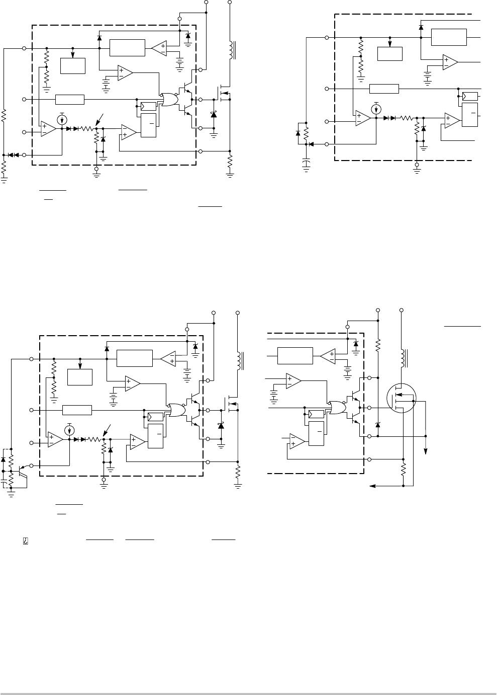
Figure 23. Current Sensing Power MOSFET
5.0V Ref
Q
Bias
Osc
EA
1.0V
5(9)
7(11)
6(10)
5(8)
3(5)
R
S
Q1
V
CC
V
in
1(1)
2(3)
4(7)
8(14)
R
1
R
2
Where: 0 V
Clamp
1.0 V
MPSA63
+
-
5.0V Ref
+
-
S
R
Q
(11)
(10)
(8)
Comp/Latch
(5)
R
S
1/4 W
V
CC
V
in
K
M
D
SENSEFET
G
S
Power Ground:
To Input Source
Return
Control Circuitry Ground:
To Pin (9)
Virtually lossless current sensing can be achieved with the implementation
of a SENSEFETt power switch. For proper operation during over-current
conditions, a reduction of the I
pk(max)
clamp level must be implemented.
Refer to Figures 20 and 22.
V
Pin5
[
R
S
I
pk
r
DS(on)
r
DM(on)
)R
S
Then : V
Pin5
[0.075I
pk
7(12)
7(12)
1.0 mA
Comp/Latch
Comp/Latch
1.0 mA
(12)
T
T
T
T
V
Clamp
V
Clamp
1.67
ǒ
R
2
R
1
) 1
Ǔ
+ 0.33x10
-3
ǒ
R
1
R
2
R
1
) R
2
Ǔ
V
Clamp
1.67
ǒ
R
2
R
1
) 1
Ǔ
t
Soft
Start
+*In
ƪ
1 *
V
C
3V
Clamp
ƫ
C
R
1
R
2
R
1
) R
2
UC3844B, UC3845B, UC2844B, UC2845B
http://onsemi.com
11
Figure 24. Current Waveform Spike Suppression
+
-
5.0V Ref
+
-
S
R
Q
7(11)
6(10)
5(8)
3(5)
R
S
Q1
V
CC
V
in
C
R
The addition of the RC filter will eliminate
instability caused by the leading edge spike
on the current waveform.
7(12)
Comp/Latch
T
Figure 25. MOSFET Parasitic Oscillations Figure 26. Bipolar Transistor Drive
+
-
S
R
5.0V Ref
Q
7(11)
6(10)
5(8)
3(5)
R
S
Q1
V
CC
V
in
Series gate resistor R
g
will damp any high frequency
parasitic oscillations caused by the MOSFET input
capacitance and any series wiring inductance in the
gate-source circuit.
6(10)
5(8)
3(5)
R
S
Q1
V
in
C1
Base Charge
Removal
The totem pole output can furnish negative base current
for enhanced transistor turn-off, with the addition of
capacitor C
1
.
I
B
+
-
0
7(12)
R
g
Comp/Latch
T
+
-
UC3844B, UC3845B, UC2844B, UC2845B
http://onsemi.com
12
+
R
2R
1.0mA
EA
2(3)
5(9)
2.5V
1(1)
R
f
C
f
R
d
R
p
From V
O
Error Amp compensation circuit for stabilizing current mode boost
and flyback topologies operating with continuous inductor current.
C
p
R
i
Figure 27. Isolated MOSFET Drive
Figure 28. Latched Shutdown
Figure 29. Error Amplifier Compensation
+
-
S
R
5.0V Ref
Q
7(11)
6(10)
5(8)
3(5)
R
S
Q1
V
CC
V
in
Isolation
Boundary
V
GS
Waveforms
+
-
0
50% DC 25% DC
ǒ
N
S
N
p
Ǔ
Bias
+
Osc
R
R
R
2R
EA
5(9)
1(1)
2(3)
4(7)
8(14)
The MCR101 SCR must be selected for a holding of < 0.5 mA @ T
A(min)
. The
simple two transistor circuit can be used in place of the SCR as shown. All
resistors are 10 k.
MCR
101
2N
3905
2N
3903
+
R
2R
1.0mA
EA
2(3)
5(9)
2.5V
1(1)
R
f
C
f
R
d
R
i
From V
O
Error Amp compensation circuit for stabilizing any current mode topology except
for boost and flyback converters operating with continuous inductor current.
R
f
8.8k
Comp/Latch
7(12)
R
C
N
S
N
P
1.0 mA
T
+
-
0
+
-
I
pk
=
V
(Pin1)
- 1.4
3 R
S

UC2844BN

Mfr. #:
Manufacturer:
STMicroelectronics
Description:
Switching Controllers 0.5mA Current Mode
Lifecycle:
New from this manufacturer.
Delivery:
DHL FedEx Ups TNT EMS
Payment:
T/T Paypal Visa MoneyGram Western Union