BZT52-G-Series
www.vishay.com
Vishay Semiconductors
Rev. 1.3, 27-Feb-13
3
Document Number: 83340
For technical questions within your region: DiodesAmericas@vishay.com
, DiodesAsia@vishay.com, DiodesEurope@vishay.com
THIS DOCUMENT IS SUBJECT TO CHANGE WITHOUT NOTICE. THE PRODUCTS DESCRIBED HEREIN AND THIS DOCUMENT
ARE SUBJECT TO SPECIFIC DISCLAIMERS, SET FORTH AT www.vishay.com/doc?91000
Notes
•I
ZT1
= 5 mA, I
ZT2
= 1 mA
(1)
Measured with pulses t
p
= 5 ms
(2)
I
ZT1
= 2.5 mA
(3)
I
ZT2
= 0.5 mA
(4)
Valid provided that electrodes are kept at ambient temperature
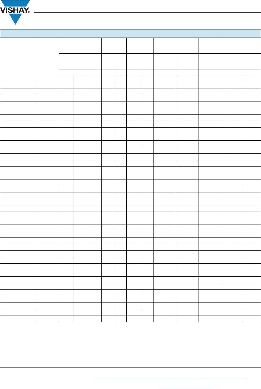
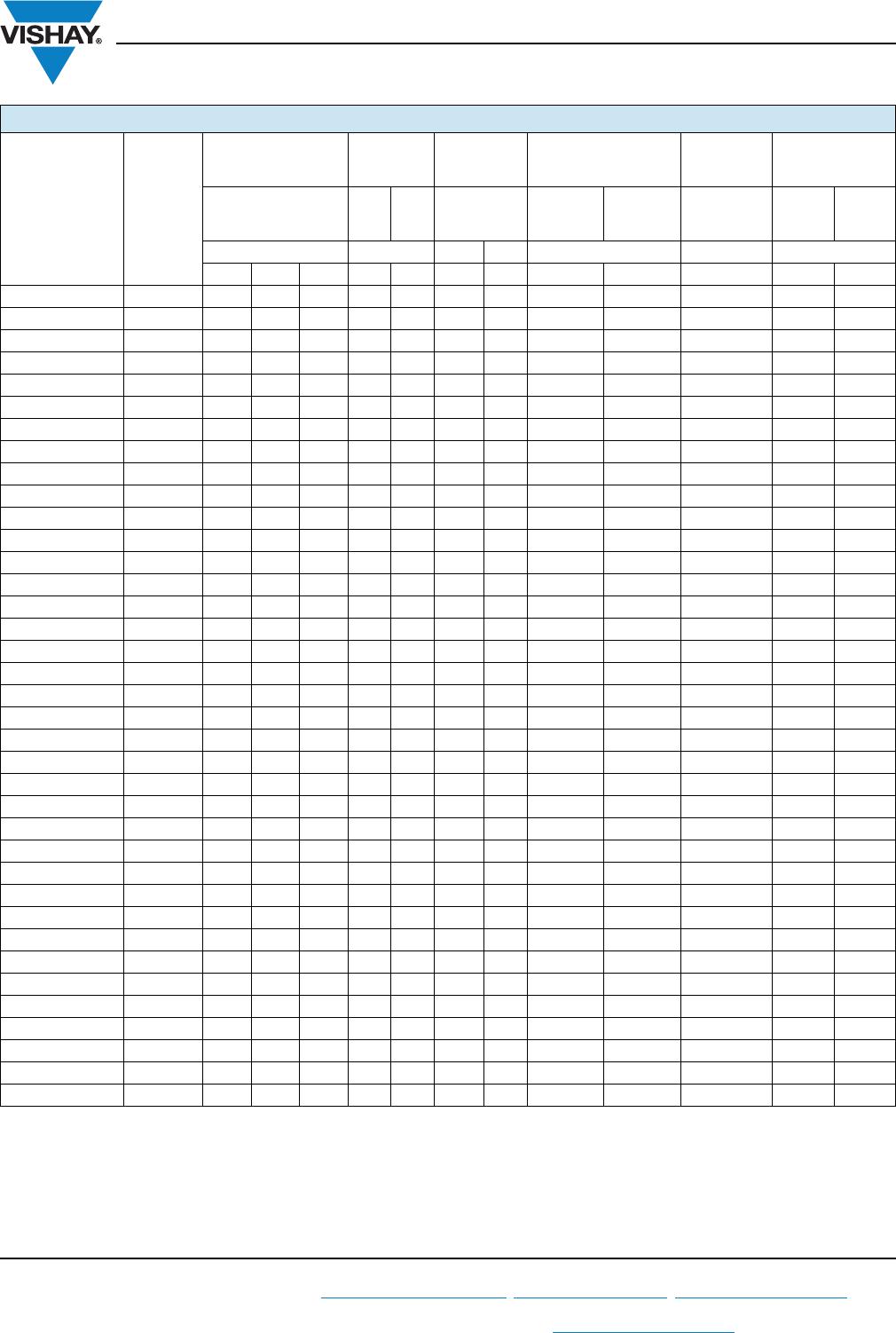
ELECTRICAL CHARACTERISTICS (T
amb
= 25 °C, unless otherwise specified)
PART NUMBER
MARKING
CODE
ZENER VOLTAGE
RANGE
(1)
TEST
CURRENT
REVERSE
VOLTAGE
DYNAMIC
RESISTANCE
TEMP.
COEFFICIENT
ADMISSABLE
ZENER
CURRENT
(4)
V
Z
at I
ZT1
I
ZT1
I
ZT2
V
R
at I
R
Z
Z
at I
ZT1
Z
ZK
at I
ZT2
VZ
I
Z
at
T
amb
=
45 °C
I
Z
at
T
amb
=
25 °C
V mA V nA 10
-4
/°C mA
MIN. NOM. MAX.
BZT52B2V4-G
V1 2.35 2.4 2.45 5 1 - 100 85 600 - 9 to - 4 - -
BZT52B2V7-G
V2 2.65 2.7 2.75 5 1 - 100 75 (< 83) < 500 - 9 to - 4 113 134
BZT52B3V0-G
V3 2.94 3.0 3.06 5 1 - 100 80 (< 95) < 500 - 9 to - 3 98 118
BZT52B3V3-G
V4 3.23 3.3 3.37 5 1 - 100 80 (< 95) < 500 - 8 to - 3 92 109
BZT52B3V6-G
V5 3.53 3.6 3.67 5 1 - 100 80 (< 95) < 500 - 8 to - 3 85 100
BZT52B3V9-G
V6 3.82 3.9 3.98 5 1 - 100 80 (< 95) < 500 - 7 to - 3 77 92
BZT52B4V3-G
V7 4.21 4.3 4.39 5 1 - 100 80 (< 95) < 500 - 6 to - 1 71 84
BZT52B4V7-G
V8 4.61 4.7 4.79 5 1 - 100 70 (< 78) < 500 - 5 to + 2 64 76
BZT52B5V1-G
V9 5 5.1 5.2 5 1 > 0.8 100 30 (< 60) < 480 - 3 to + 4 56 67
BZT52B5V6-G
VA 5.49 5.6 5.71 5 1 > 1 100 10 (< 40) < 400 - 2 to + 6 50 59
BZT52B6V2-G
VB 6.08 6.2 6.32 5 1 > 2 100 4.8 (< 10) < 200 - 1 to + 7 45 54
BZT52B6V8-G
VC 6.66 6.8 6.94 5 1 > 3 100 4.5 (< 8) < 150 + 2 to + 7 41 49
BZT52B7V5-G
VD 7.35 7.5 7.65 5 1 > 5 100 4 (< 7) < 50 + 3 to + 7 37 44
BZT52B8V2-G
VE 8.04 8.2 8.36 5 1 > 6 100 4.5 (< 7) < 50 + 4 to + 7 34 40
BZT52B9V1-G
VF 8.92 9.1 9.28 5 1 > 7 100 4.8 (< 10) < 50 + 5 to + 8 30 36
BZT52B10-G
VG 9.8 10 10.2 5 1 > 7.5 100 5.2 (< 15) < 70 + 5 to + 8 28 33
BZT52B11-G
VH 10.8 11 11.2 5 1 > 8.5 100 6 (< 20) < 70 + 5 to + 9 25 30
BZT52B12-G
VI 11.8 12 12.2 5 1 > 9 100 7 (< 20) < 90 + 6 to + 9 23 28
BZT52B13-G
VK 12.7 13 13.3 5 1 > 10 100 9 (< 25) < 110 + 7 to + 9 21 25
BZT52B15-G
VL 14.7 15 15.3 5 1 > 11 100 11 (< 30) < 110 + 7 to + 9 19 23
BZT52B16-G
VM 15.7 16 16.3 5 1 > 12 100 13 (< 40) < 170 + 8 to + 9.5 17 20
BZT52B18-G
VN 17.6 18 18.4 5 1 > 14 100 18 (< 50) < 170 + 8 to + 9.5 15 18
BZT52B20-G
VO 19.6 20 20.4 5 1 > 15 100 20 (< 50) < 220 + 8 to + 10 14 17
BZT52B22-G
VP 21.6 22 22.4 5 1 > 17 100 25 (< 55) < 220 + 8 to + 10 13 16
BZT52B24-G
VR 23.5 24 24.5 5 1 > 18 100 28 (< 80) < 220 + 8 to + 10 11 13
BZT52B27-G
VS 26.5 27 27.5 5 1 > 20 100 30 (< 80) < 250 + 8 to + 10 10 12
BZT52B30-G
VT 29.4 30 30.6 5 1 > 22.5 100 35 (< 80) < 250 + 8 to + 10 9 10
BZT52B33-G
VU 32.3 33 33.7 5 1 > 25 100 40 (< 80) < 250 + 8 to + 10 8 9
BZT52B36-G
VW 35.3 36 36.7 5 1 > 27 100 40 (< 90) < 250 + 8 to + 10 8 9
BZT52B39-G
VX 38.2 39 39.8 5 1 > 29 100 50 (< 90) < 300 + 10 to + 12 7 8
BZT52B43-G
VY 42.1 43 43.9 5 1 > 32 100 60 (< 100) < 700 + 10 to + 12 6 7
BZT52B47-G
VZ 46.1 47 47.9 5 1 > 35 100 70 (< 100) < 750 + 10 to + 12 5 6
BZT52B51-G
U1 50 51 52 5 1 > 38 100 70 (< 100) < 750 + 10 to + 12 5 6
BZT52B56-G
U2 54.9 56 57.1 2.5 1 - 100 < 135
(2)
< 1000
(3)
typ. + 10
(2)
--
BZT52B62-G
U3 60.8 62 63.2 2.5 1 - 100 < 150
(2)
< 1000
(3)
typ. + 10 (
2)
--
BZT52B68-G
U4 66.6 68 69.4 2.5 1 - 100 < 200
(2)
< 1000
(3)
typ. + 10
(2)
--
BZT52B75-G
U5 73.5 75 76.5 2.5 1 - 100 < 250
(2))
< 1500
(3)
typ. + 10
(2)
--