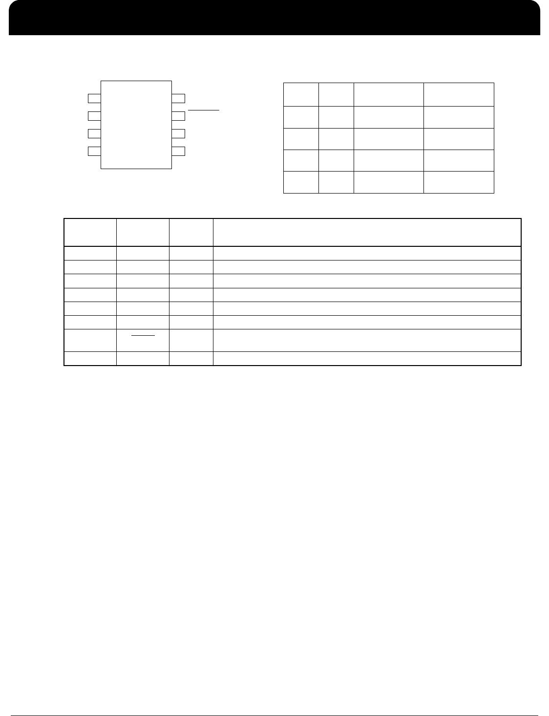
341MPLFT

DATASHEET
FIELD PROGRAMMABLE SS VERSACLOCK SYNTHESIZER ICS341
IDT® / ICS™
FIELD PROGRAMMABLE SS VERSACLOCK SYNTHESIZER 1
ICS341 REV N 072816
Description
The ICS341 is a low cost, single-output, field programmable
clock synthesizer. The ICS341 can generate an output
frequency from 250 kHz to 200 MHz and may employ
Spread Spectrum techniques to reduce system
electro-magnetic interference (EMI).
Using IDT’s VersaClock
software to configure the PLL and
output, the ICS341 contains a One-Time Programmable
(OTP) ROM to allow field programmability. Programming
features include 4 selectable configuration registers.
The device employs Phase-Locked Loop (PLL) techniques
to run from a standard fundamental mode, inexpensive
crystal, or clock. It can replace multiple crystals and
oscillators, saving board space and cost.
The device also has a power-down feature that tri-states the
clock outputs and turns off the PLLs when the PDTS
pin is
taken low.
The ICS341 is also available in factory programmed custom
versions for high-volume applications.
Features
8-pin SOIC package (Pb-free)
Highly accurate frequency generation
M/N Multiplier PLL: M = 1...2048, N = 1...1024
Output clock frequencies up to 200 MHz
Four ROM locations for frequency and spread selection
Spread spectrum capability for lower system EMI
Center or Down Spread up to 4% total
Selectable 32 kHz or 120 kHz modulation
Input crystal frequency from 5 to 27 MHz
Input clock frequency from 2 to 50 MHz
Operating voltage of 3.3 V
Advanced, low-power CMOS process
For two output clocks, use the ICS342. For three output
clocks, see the ICS343. For more than three outputs, see
the ICS345 or ICS348.
Block Diagram
Crystal
Oscillator
PLL Clock Synthesis,
Spred Spectrum and
Control Circuitry
CLK
PDTS (output and PLL)
OTP ROM
with PLL
Divider
Values
S1:0
2
VDD
GND
X2
Crystal or
clock input
External capacitors are
required with a crystal input.
X1/ICLK
ICS341
FIELD PROGRAMMABLE SS VERSACLOCK SYNTHESIZER EPROM CLOCK SYNTHESIZER
IDT® / ICS™
FIELD PROGRAMMABLE SS VERSACLOCK SYNTHESIZER 2
ICS341 REV N 072816
Pin Assignment
8-pin (150 mil) SOIC
Output Clock Selection Table
Pin Descriptions
External Components
Series Termination Resistor
Clock output traces over one inch should use series
termination. To series terminate a 50 trace (a commonly
used trace impedance), place a 33 resistor in series with
the clock line, as close to the clock output pin as possible.
The nominal impedance of the clock output is 20.
Decoupling Capacitor
As with any high-performance mixed-signal IC, the ICS341
must be isolated from system power supply noise to perform
optimally.
A decoupling capacitor of 0.01µF must be connected
between VDD and the PCB ground plane.
Crystal Load Capacitors
The device crystal connections should include pads for
small capacitors from X1 to ground and from X2 to ground.
These capacitors are used to adjust the stray capacitance of
the board to match the nominally required crystal load
capacitance. Because load capacitance can only be
increased in this trimming process, it is important to keep
stray capacitance to a minimum by using very short PCB
traces (and no vias) between the crystal and device. Crystal
capacitors must be connected from each of the pins X1 and
X2 to ground.
The value (in pF) of these crystal caps should equal (C
L
-6
pF)*2. In this equation, C
L
= crystal load capacitance in pF.
Example: For a crystal with a 16 pF load capacitance, each
crystal capacitor would be 20 pF [(16-6) x 2] = 20.
PCB Layout Recommendations
For optimum device performance and lowest output phase
noise, the following guidelines should be observed.
1) The 0.01µF decoupling capacitor should be mounted on
the component side of the board as close to the VDD pin as
possible. No vias should be used between the decoupling
capacitor and VDD pin. The PCB trace to VDD pin should be
kept as short as possible, as should the PCB trace to the
ground via. Distance of the ferrite bead and bulk decoupling
from the device is less critical.
2) The external crystal should be mounted just next to the
device with short traces. The X1 and X2 traces should not
be routed next to each other with minimum spaces, instead
they should be separated and away from other traces.
X1/ICLK
VDD
GND
PDTS
S0
S1
CLK
X2
1
2
3
4
8
7
6
5
S1 S0 CLK (MHz) Spread
Percentage
0 0 User
Configurable
User
Configurable
01 User
Configurable
User
Configurable
10 User
Configurable
User
Configurable
11 User
Configurable
User
Configurable
Pin
Number
Pin
Name
Pin
Type
Pin Description
1 X1/ICLK XI Connect this pin to a crystal or external clock input.
2 VDD Power Connect to +3.3 V.
3 GND Power Connect to ground.
4 S0 Input Select pin 0 for frequency selection on CLK. Internal pull-up resistor.
5 CLK Output Clock output. Weak internal pull-down when tri-state.
6 S1 Input Select pin 1 for frequency selection on CLK. Internal pull-up resistor.
7PDTS
Input
Powers down entire chip. Tri-states CLK outputs when low. Internal pull-up
resistor.
8 X2 XO Connect this pin to a crystal, or float for clock input.
ICS341
FIELD PROGRAMMABLE SS VERSACLOCK SYNTHESIZER EPROM CLOCK SYNTHESIZER
IDT® / ICS™
FIELD PROGRAMMABLE SS VERSACLOCK SYNTHESIZER 3
ICS341 REV N 072816
3) To minimize EMI, the 33 series termination resistor (if
needed) should be placed close to the clock output.
4) An optimum layout is one with all components on the
same side of the board, minimizing vias through other signal
layers. Other signal traces should be routed away from the
ICS341. This includes signal traces just underneath the
device, or on layers adjacent to the ground plane layer used
by the device.
ICS341 Configuration Capabilities
The architecture of the ICS341 allows the user to easily
configure the device to a wide range of output frequencies,
for a given input reference frequency.
The frequency multiplier PLL provides a high degree of
precision. The M/N values (the multiplier/divide values
available to generate the target VCO frequency) can be set
within the range of M = 1 to 2048 and N = 1 to 1024.
The ICS341 also provides separate output divide values,
from 2 through 20, to allow the two output clock banks to
support widely differing frequency values from the same
PLL.
Each output frequency can be represented
as:
IDT VersaClock Software
IDT applies years of PLL optimization experience into a user
friendly software that accepts the user’s target reference
clock and output frequencies and generates the lowest jitter,
lowest power configuration, with only a press of a button.
The user does not need to have prior PLL experience or
determine the optimal VCO frequency to support multiple
output frequencies.
VersaClock software quickly evaluates accessible VCO
frequencies with available output divide values and provides
an easy to understand, bar code rating for the target output
frequencies. The user may evaluate output accuracy,
performance trade-off scenarios in seconds.
Spread Spectrum Modulation
The ICS341 utilizes frequency modulation (FM) to distribute
energy over a range of frequencies. By modulating the
output clock frequencies, the device effectively lowers
energy across a broader range of frequencies; thus,
lowering a system’s electro-magnetic interference (EMI).
The modulation rate is the time from transitioning from a
minimum frequency to a maximum frequency and then back
to the minimum.
Spread Spectrum Modulation can be applied as either
“center spread” or “down spread”. During center spread
modulation, the deviation from the target frequency is equal
in the positive and negative directions. The effective average
frequency is equal to the target frequency. In applications
where the clock is driving a component with a maximum
frequency rating, down spread should be applied. In this
case, the maximum frequency, including modulation, is the
target frequency. The effective average frequency is less
than the target frequency.
The ICS341 operates in both center spread and down
spread modes. For center spread, the frequency can be
modulated between +/- 0.125% to +/-2.0%. For down
spread, the frequency can be modulated between -0.25% to
-4.0%.
Both output frequency banks will utilize identical spread
spectrum percentage deviations and modulation rates, if a
common VCO frequency can be identified.
Spread Spectrum Modulation Rate
The spread spectrum modulation frequency applied to the
output clock frequency may occur at a variety of rates. For
applications requiring the driving of “down-circuit” PLLs,
Zero Delay Buffers, or those adhering to PCI standards, the
spread spectrum modulation rate should be set to 30-33
kHz. For other applications, a 120 kHz modulation option is
available.
Using VersaClock Products with an Input Clock
Source
In order to ensure proper startup with an input clock rather
than a crystal, the supply voltage must be within the
operating range (3.3V ±10%) and the input signal must be
stable and free from glitching. The input clock must provide
pulses of at least 20ns, and no more than 500ns, for at least
160 clock cycles without any interruptions to the clock or
power during this period. It may take up to 4ms for output
frequencies to reach their target frequency values.
An alternative method is to have the PDTS
pin asserted low
while power supplies and clock sources stabilize.Once the
power supply and input clock source are constant and within
the acceptable frequency range, bring PDTS
high. This
approach is preferred if the clock source is derived from
another PLL, or the source oscillator produces
unpredictable output pulses prior to stabilization. No
considerations need to be taken when using a crystal input
source with VersaClock products.
OutputFreq
REFFreq
OutputDivide
--------------------------------------
M
N
-----
=

341MPLFT

Mfr. #:
Manufacturer:
IDT
Description:
Clock Synthesizer / Jitter Cleaner FIELD PROGRAMMABLE S S VERSACLOCK SYNTHES
Lifecycle:
New from this manufacturer.
Delivery:
DHL FedEx Ups TNT EMS
Payment:
T/T Paypal Visa MoneyGram Western Union

Products related to this Datasheet