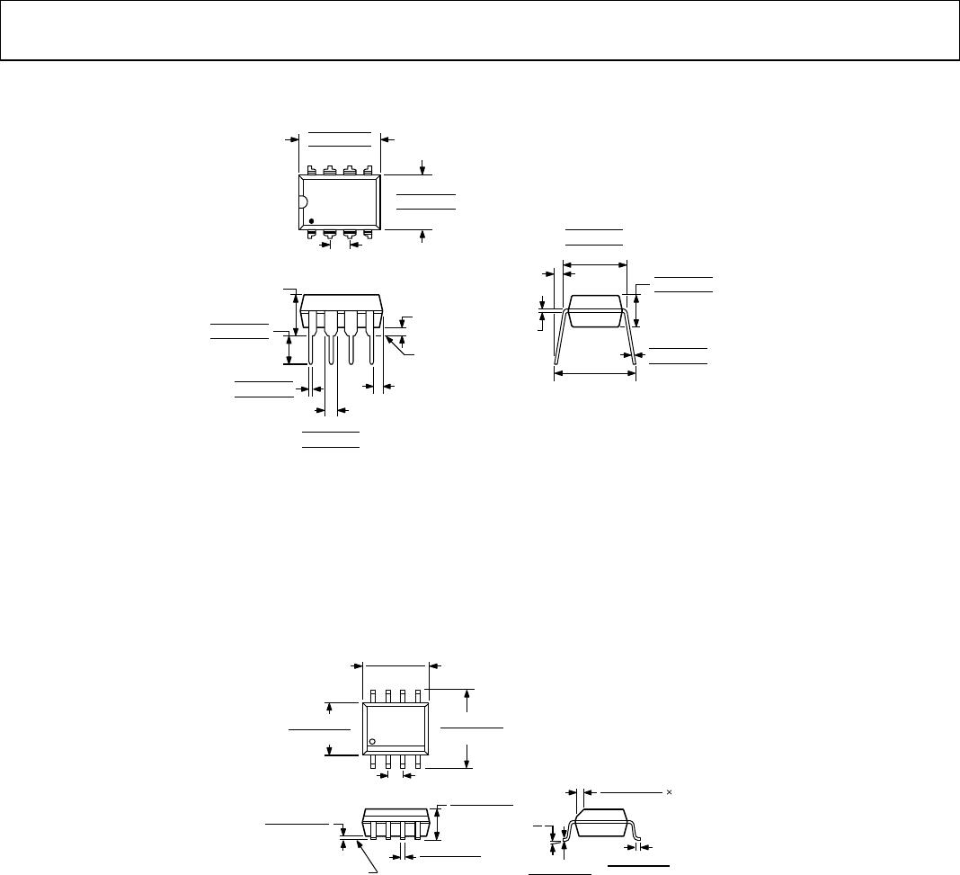
AD654
–10–
REV.
8
7
6
5
1
2
3
4
AD654
68kV
1kV
V
IN
(0V TO 1V)
C
T
100pF
+5V
0.1mF
0.1mF
R
T
= 1kV
+
–
A
J270
J270
Q1
Q2
MINIMUM
DISTANCE
+15V
V1
68kV
V2
10mF
10mF
+
5.9kV
1%
(32)
R7
8.2V
MINIMUM
DISTANCE
0.1mF
10mF
D
–5V
V3
A3-a
A3-b
18V
470pF
A3-c
A3-d
V4
A3 = 74LS86
A2
LM360
D
10mF
0.1mF
+15V
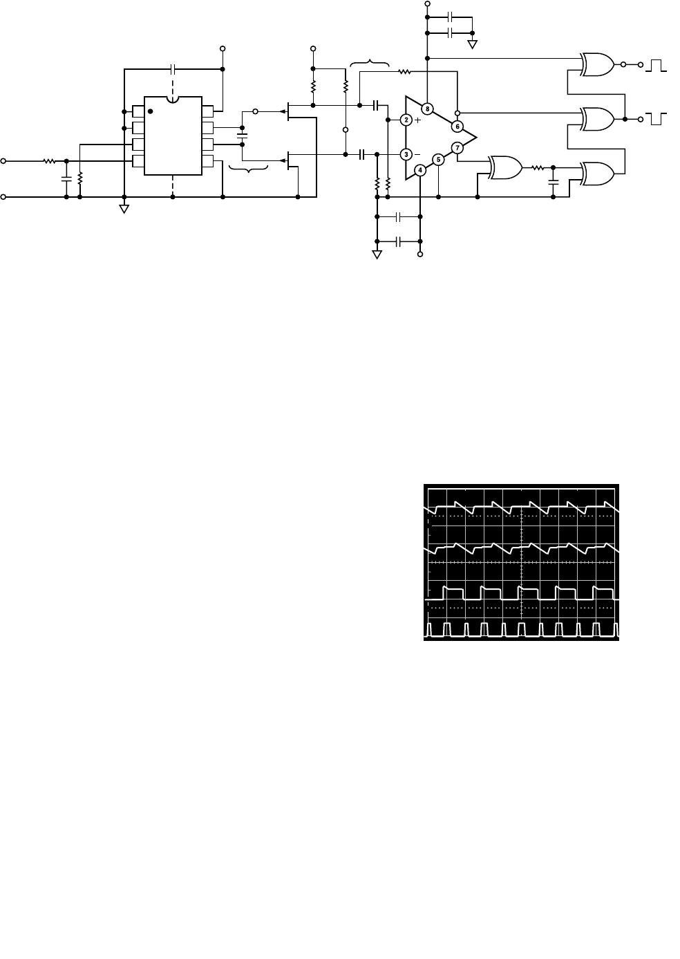
Figure 13. 2 MHz, Frequency Doubling V/F
OPERATION AT HIGHER OUTPUT FREQUENCIES
Operation of the AD654 via the conventional output (Pins 1 and
2) is speed limited to approximately 500 kHz for reasons of TTL
logic compatibility. Although the output stage may become
speed limited, the multivibrator core itself is able to oscillate to
1 MHz or more. The designer may take advantage of this feature in
order to operate the device at frequencies in excess of 500 kHz.
Figure 13 illustrates this with a circuit offering 2 MHz full scale.
In this circuit the AD654 is operated at a full scale (FS) of 1 mA,
with a C
T
of 100 pF. This achieves a basic device FS frequency
of 1 MHz across C
T
. The P channel JFETs, Q1 and Q2, buffer
the differential timing capacitor waveforms to a low impedance
level where the push-pull signal is then ac coupled to the high speed
comparator A2. Hysteresis is used, via R7, for nonambiguous
switching and to eliminate the oscillations which would other-
wise occur at low frequencies.
The net result of this is a very high speed circuit which does not
compromise the AD654 dynamic range. This is a result of the FET
buffers typically having only a few pA of bias current. The high
end dynamic range is limited, however, by parasitic package and
layout capacitances in shunt with C
T
, as well as those from each node
to ac ground. Minimizing the lead length between A2–6/A2–7 and
Q1/Q2 in PC layout will help. A ground plane will also help
stability. Figure 14 shows the waveforms V1–V4 found at the
respective points shown in Figure 13.
The output of the comparator is a complementary square wave
at 1 MHz FS. Unlike pulse train output V/F converters, each
half-cycle of the AD654 output conveys information about the
input. Thus it is possible to count edges, rather than full cycles
of the output, and double the effective output frequency. The
XOR gate following A2 acts as an edge detector producing a short
pulse for each input state transition. This effectively doubles the
V/F FS frequency to 2 MHz. The final result is a 1 V full-scale
input V/F with a 2 MHz full-scale output capability; typical
nonlinearity is 0.5%.
100
90
10
0%
500ns
2V 5V
2V 5V
2V
0
2V
0
5V
0
5V
0
V1
V2
V3
V4
Figure 14. Waveforms of 2 MHz Frequency Doubler