VS-STPS20L15G-M3
www.vishay.com
Vishay Semiconductors
Revision: 06-Nov-17
1
Document Number: 96397
For technical questions within your region: DiodesAmericas@vishay.com
, DiodesAsia@vishay.com, DiodesEurope@vishay.com
THIS DOCUMENT IS SUBJECT TO CHANGE WITHOUT NOTICE. THE PRODUCTS DESCRIBED HEREIN AND THIS DOCUMENT
ARE SUBJECT TO SPECIFIC DISCLAIMERS, SET FORTH AT www.vishay.com/doc?91000
High Performance Schottky Rectifier, 20 A
FEATURES
• 125 °C T
J
operation (V
R
< 5 V)
• Center tap module
• Optimized for OR-ing applications
• Ultralow forward voltage drop
• High frequency operation
• Guard ring for enhanced ruggedness and long term
reliability
• High purity, high temperature epoxy encapsulation for
enhanced mechanical strength and moisture resistance
• Meets MSL level 1, per J-STD-020, LF maximum peak
of 245 °C
• Designed and qualified according to JEDEC
®
-JESD 47
• Material categorization: for definitions of compliance
please see www.vishay.com/doc?99912
DESCRIPTION
The Schottky rectifier module has been optimized for
ultra low forward voltage drop specifically for the OR-ing
of parallel power supplies. The proprietary barrier
technology allows for reliable operation up to 125 °C
junction temperature. Typical applications are in parallel
switching power supplies, converters, reverse battery
protection, and redundant power subsystems.
PRIMARY CHARACTERISTICS
I
F(AV)
20 A
V
R
15 V
V
F
at I
F
0.33 V
I
RM
max. 600 mA at 100 °C
T
J
max. 125 °C
E
AS
10 mJ
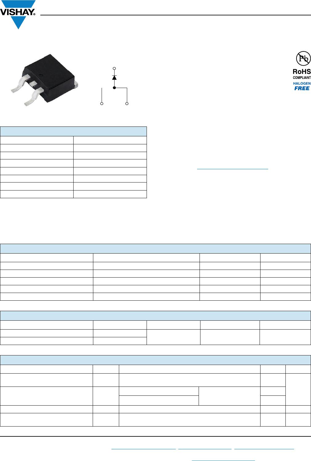
Package D
2
PAK (TO-263AB)
Circuit configuration Single
Anode
1
3
Base
cathode
2
N/C
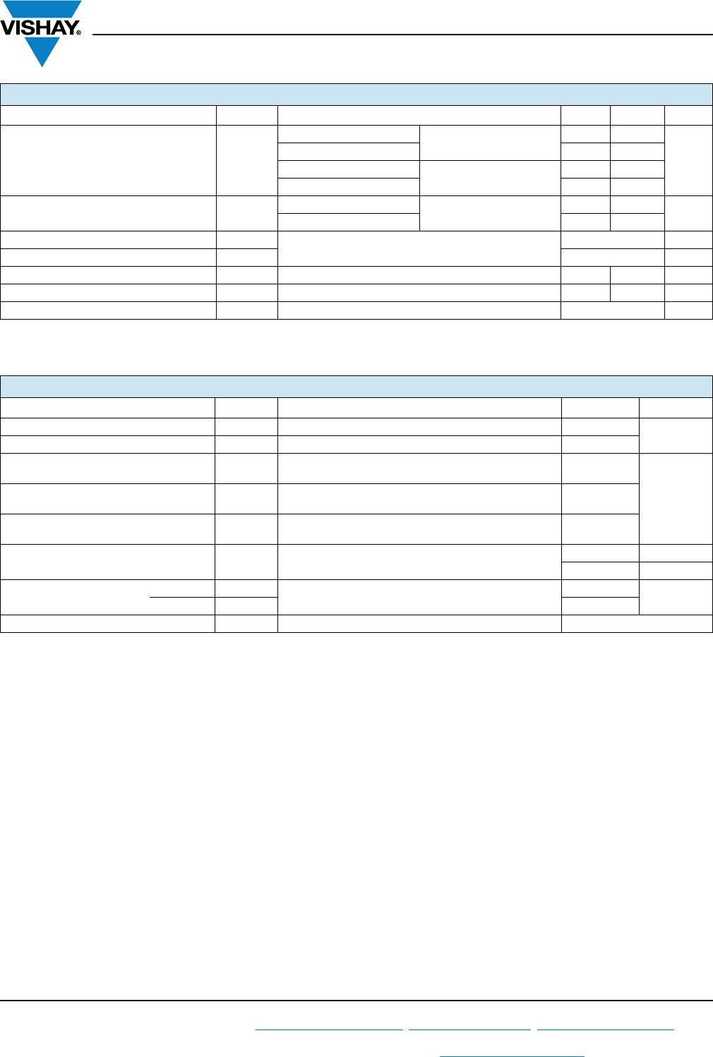
MAJOR RATINGS AND CHARACTERISTICS
SYMBOL CHARACTERISTICS VALUES UNITS
I
F(AV)
Rectangular waveform 20 A
V
RRM
15 V
I
FSM
t
p
= 5 μs sine 700 A
V
F
19 A
pk
, T
J
= 125 °C (typical) 0.25 V
T
J
Range -55 to +125 °C
VOLTAGE RATINGS
PARAMETER SYMBOL TEST CONDITIONS VS-STPS20L15G-M3 UNITS
Maximum DC reverse voltage V
R
T
J
= 100 °C 15 V
Maximum working peak reverse voltage V
RWM
ABSOLUTE MAXIMUM RATINGS
PARAMETER SYMBOL TEST CONDITIONS VALUES UNITS
Maximum average forward current
See fig. 5
I
F(AV)
50 % duty cycle at T
C
= 85 °C, rectangular waveform 20
A
Maximum peak one cycle
non-repetitive surge current
See fig. 7
I
FSM
5 μs sine or 3 μs rect. pulse
Following any rated load
condition and with rated
V
RRM
applied
700
10 ms sine or 6 ms rect. pulse 330
Non-repetitive avalanche energy E
AS
T
J
= 25 °C, I
AS
= 2 A, L = 6 mH 10 mJ
Repetitive avalanche current I
AR
Current decaying linearly to zero in 1 μs
Frequency limited by T
J
maximum V
A
= 1.5 x V
R
typical
2A