5©2015 Integrated Device Technology, Inc Revision E December 2, 2015
85304-01 Data Sheet
Table 4D. LVPECL DC Characteristics, V
CC
= 3.3V ± 5%, V
EE
=0V, T
A
= 0°C to 70°C
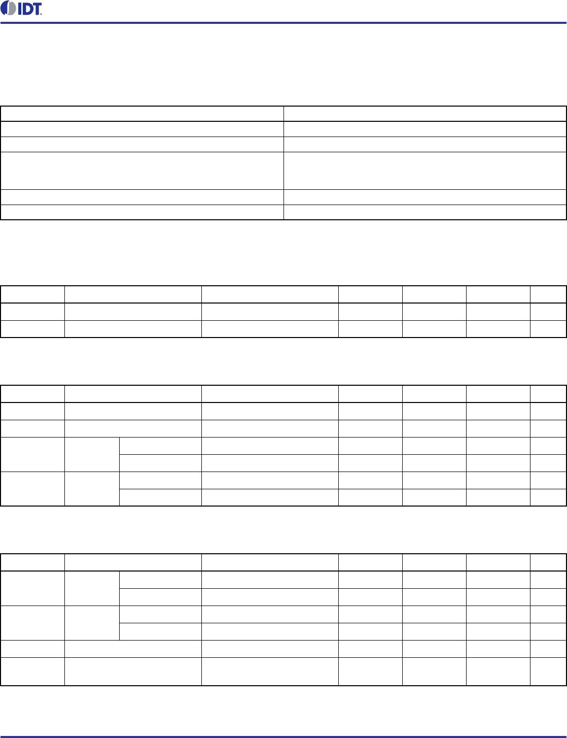
NOTE 1: Outputs terminated with 50 to V
CC
– 2V.
AC Electrical Characteristics
Table 5. AC Characteristics, V
CC
= 3.3V ± 5%, V
EE
=0V, T
A
= 0°C to 70°C
NOTE: Electrical parameters are guaranteed over the specified ambient operating temperature range, which is established when the device is
mounted in a test socket with maintained transverse airflow greater than 500 lfpm. The device will meet specifications after thermal equilibrium
has been reached under these conditions.
NOTE: All parameters measured at 500MHz unless noted otherwise
NOTE: The cycle-to-cycle jitter on the input will equal the jitter on the output. The part does not add jitter.
NOTE 1: Measured from the differential input crossing point to the differential output crossing point. Measured at the output differential cross
points.
NOTE 2: Defined as skew between outputs at the same supply voltage and with equal load conditions. Measured at the output differential
cross points.
NOTE 3: This parameter is defined in accordance with JEDEC Standard 65.
NOTE 4: Defined as skew between outputs on different devices operating at the same supply voltage, same frequency, same temperature and
with equal load conditions. Using the same type of inputs on each device, the outputs are measured at the differential cross points.
Symbol Parameter Test Conditions Minimum Typical Maximum Units
V
OH
Output High Current; NOTE 1 V
CC
– 1.4 V
CC
– 1.0 µA
V
OL
Output Low Current; NOTE 1 V
CC
– 2.0 V
CC
– 1.7 µA
V
SWING
Peak-to-Peak Output Voltage
Swing
0.6 0.85 V
Symbol Parameter Test Conditions Minimum Typical Maximum Units
f
OUT
Output Frequency 650 MHz
t
PD
Propagation Delay; NOTE 1 ƒ 650MHz 1.0 2.1 ns
tsk(o) Output Skew; NOTE 2, 3 35 ps
tsk(pp) Part-to-Part Skew; NOTE 3, 4 150 ps
t
R
/ t
F
Output Rise/Fall Time 20% to 80% @ 50MHz 300 700 ps
odc Output Duty Cycle 48 50 52 %