NCP3520/NCP3521
http://onsemi.com
3
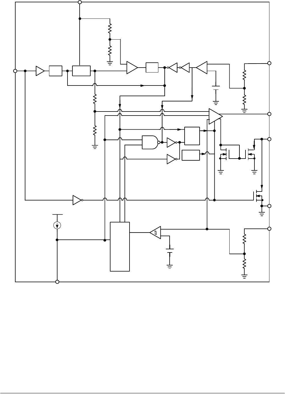
PACKAGE PIN DESCRIPTION Micro8
Pin # Symbol Description
1 NRCS Non Rush current on Startup. Capacitor to ground controls output voltage slew rate and short circuit
delay time.
2 GND Ground.
3 EN Enable input control.
4 VCC Power Supply Voltage Input.
5 VFB Voltage Feedback pin into the error amplifier for maintaining the output voltage.
6 VS Source input. Provides pulldown capability (1.2 mA operating & 220 mA turnoff) for fast output voltage
response time.
7 G Gate Drive for the external NFET.
8 VD NFET Drain input for voltage sensing.
MAXIMUM RATINGS
Rating Value Unit
All Pins -0.3 to 7 V
IG (DC)
IG (AC)
IVS (DC)
10
10
300
mA
Electrostatic Discharge, Human Body Model 1.5 kV
Electrostatic Discharge, Machine Model 100 V
Package Thermal Resistance
Micro8 238 °C/W
Operating Junction Temperature -10 to 150 °C
Storage Temperature Range -55 to 150 °C
Stresses exceeding Maximum Ratings may damage the device. Maximum Ratings are stress ratings only. Functional operation above the
Recommended Operating Conditions is not implied. Extended exposure to stresses above the Recommended Operating Conditions may affect
device reliability.
ELECTRICAL CHARACTERISTICS (T
J
= 25°C, V
CC
= 5 V, V
D
= 2.0 V, EN = 3 V, External FET = NTMS4107N (Note 3), unless
otherwise specified)
Characteristic Conditions Min Typ Max Unit
REGULATOR OUTPUT
Feedback Voltage (NCP3520) I
O
(NTMS4107N) = 50 mA
4.5 V < V
CC
< 5.5 V, 0°C < T
J
< 100°C
(Note 1)
1.188
1.176
1.200
1.200
1.212
1.224
V
V
Feedback Voltage (NCP3521) I
O
(NTMS4107N) = 50 mA
4.5 V < V
CC
< 5.5V, 0°C < T
J
< 100°C
(Note 1)
1.485
1.470
1.500
1.500
1.515
1.530
V
V
Supply Current
Sleep Mode
Run Mode
Short Circuit Latch Condition
EN = 0 V
EN = 3 V
EN = 3 V
-
-
-
0
1.25
0.5
10
1.7
1.7
mA
mA
mA
Line Regulation (NCP3520) 4.5 V < V
CC
< 5.5 V, I
OUT
= 0
4.5 V < V
CC
< 5.5 V, I
OUT
= 3 A (Note 1)
- 1.2
1.2
6.0
6.0
mV
mV
Line Regulation (NCP3521) 4.5 V < V
CC
< 5.5 V, I
OUT
= 0
4.5 V < V
CC
< 5.5 V, I
OUT
= 3 A (Note 1)
- 1.5
1.5
7.5
7.5
mV
mV
Load Regulation (Note 2) I
O
= 0 A to 3 A - 0.50 10 mV
1. Guaranteed by Design
2. Load regulation may vary with the selection of an external FET other than the NTMS4107N.
3. See “External Components” section on Page 8.