VS-16TTS08STRR-M3

VS-16TTS08S-M3, VS-16TTS12S-M3 Series
www.vishay.com
Vishay Semiconductors
Revision: 04-Jan-18
1
Document Number: 96412
For technical questions within your region: DiodesAmericas@vishay.com
, DiodesAsia@vishay.com, DiodesEurope@vishay.com
THIS DOCUMENT IS SUBJECT TO CHANGE WITHOUT NOTICE. THE PRODUCTS DESCRIBED HEREIN AND THIS DOCUMENT
ARE SUBJECT TO SPECIFIC DISCLAIMERS, SET FORTH AT www.vishay.com/doc?91000
Thyristor High Voltage, Surface Mount Phase Control SCR, 16 A
FEATURES
Meets MSL level 1, per J-STD-020,
LF maximum peak of 245 °C
Designed and qualified according
JEDEC
®
-JESD 47
Material categorization: for definitions of
compliance please see www.vishay.com/doc?99912
APPLICATIONS
Input rectification (soft start)
Vishay input diodes, switches and output rectifiers which
are available in identical package outlines
DESCRIPTION
The VS-16TTS..S-M3 high voltage series of silicon
controlled rectifiers are specifically designed for medium
power switching and phase control applications. The glass
passivation technology used has reliable operation up to
125 °C junction temperature.
Note
•T
A
= 55 °C, T
J
= 125 °C, footprint 300 mm
2
PRIMARY CHARACTERISTICS
I
T(AV)
10 A
V
DRM
/V
RRM
800 V, 1200 V
V
TM
1.4 V
I
GT
60 mA
T
J
-40 °C to 125 °C
Package D
2
PAK (TO-263AB)
Circuit configuration Single SCR
3
Gate
2, 4
Anode
1
Cathode
D
2
PAK (TO-263AB)
1
2
3
OUTPUT CURRENT IN TYPICAL APPLICATIONS
APPLICATIONS SINGLE-PHASE BRIDGE THREE-PHASE BRIDGE UNITS
NEMA FR-4 or G-10 glass fabric-based epoxy
with 4 oz. (140 μm) copper
2.5 3.5
A
Aluminum IMS, R
thCA
= 15 °C/W 6.3 9.5
Aluminum IMS with heatsink, R
thCA
= 5 °C/W 14.0 18.5
MAJOR RATINGS AND CHARACTERISTICS
PARAMETER TEST CONDITIONS VALUES UNITS
I
T(AV)
Sinusoidal waveform 10
A
I
RMS
16
V
RRM
/V
DRM
800 to 1200 V
I
TSM
200 A
V
T
10 A, T
J
= 25 °C 1.4 V
dV/dt 500 V/μs
dI/dt 150 A/μs
T
J
-40 to +125 °C
VOLTAGE RATINGS
PART NUMBER
V
RRM
, MAXIMUM PEAK
REVERSE VOLTAGE
V
V
DRM
, MAXIMUM PEAK
DIRECT VOLTAGE
V
I
RRM
/I
DRM
AT 125 °C
mA
VS-16TTS08S-M3 800 800
10
VS-16TTS12S-M3 1200 1200
VS-16TTS08S-M3, VS-16TTS12S-M3 Series
www.vishay.com
Vishay Semiconductors
Revision: 04-Jan-18
2
Document Number: 96412
For technical questions within your region: DiodesAmericas@vishay.com
, DiodesAsia@vishay.com, DiodesEurope@vishay.com
THIS DOCUMENT IS SUBJECT TO CHANGE WITHOUT NOTICE. THE PRODUCTS DESCRIBED HEREIN AND THIS DOCUMENT
ARE SUBJECT TO SPECIFIC DISCLAIMERS, SET FORTH AT www.vishay.com/doc?91000
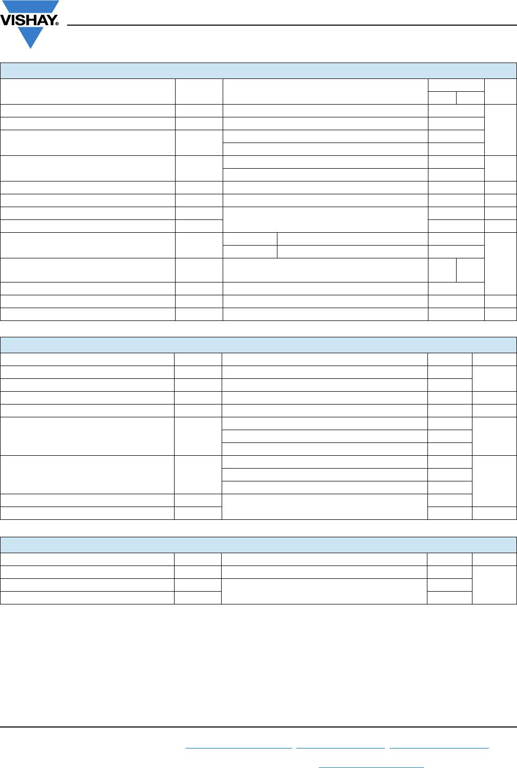
ABSOLUTE MAXIMUM RATINGS
PARAMETER SYMBOL TEST CONDITIONS
VALUES
UNITS
TYP. MAX.
Maximum average on-state current I
T(AV)
T
C
= 98 °C, 180° conduction, half sine wave 10
A
Maximum RMS on-state current I
RMS
16
Maximum peak, one-cycle,
non-repetitive surge current
I
TSM
10 ms sine pulse, rated V
RRM
applied 170
10 ms sine pulse, no voltage reapplied 200
Maximum I
2
t for fusing I
2
t
10 ms sine pulse, rated V
RRM
applied 144
A
2
s
10 ms sine pulse, no voltage reapplied 200
Maximum I
2
t for fusing I
2
t t = 0.1 ms to 10 ms, no voltage reapplied 2000 A
2
s
Maximum on-state voltage drop V
TM
10 A, T
J
= 25 °C 1.4 V
On-state slope resistance r
t
T
J
= 125 °C
24.0 m
Threshold voltage V
T(TO)
1.1 V
Maximum reverse and direct leakage current I
RM
/I
DM
T
J
= 25 °C V
R
= rated V
RRM
/V
DRM
0.5
mA
T
J
= 125 °C 10
Holding current I
H
Anode supply = 6 V, resistive load, initial I
T
= 1 A,
T
J
= 25 °C
- 150
Maximum latching current I
L
Anode supply = 6 V, resistive load,T
J
= 25 °C 200
Maximum rate of rise of off-state voltage dV/dt T
J
= T
J
max. linear to 80 % V
DRM
= R
g
- k = open 500 V/μs
Maximum rate of rise of turned-on current dI/dt 150 A/μs
TRIGGERING
PARAMETER SYMBOL TEST CONDITIONS VALUES UNITS
Maximum peak gate power P
GM
8.0
W
Maximum average gate power P
G(AV)
2.0
Maximum peak positive gate current + I
GM
1.5 A
Maximum peak negative gate voltage - V
GM
10 V
Maximum required DC gate current to trigger I
GT
Anode supply = 6 V, resistive load, T
J
= - 10 °C 90
mAAnode supply = 6 V, resistive load, T
J
= 25 °C 60
Anode supply = 6 V, resistive load, T
J
= 125 °C 35
Maximum required DC gate voltage to trigger V
GT
Anode supply = 6 V, resistive load, T
J
= - 10 °C 3.0
V
Anode supply = 6 V, resistive load, T
J
= 25 °C 2.0
Anode supply = 6 V, resistive load, T
J
= 125 °C 1.0
Maximum DC gate voltage not to trigger V
GD
T
J
= 125 °C, V
DRM
= Rated value
0.25
Maximum DC gate current not to trigger I
GD
2.0 mA
SWITCHING
PARAMETER SYMBOL TEST CONDITIONS VALUES UNITS
Typical turn-on time t
gt
T
J
= 25 °C 0.9
μsTypical reverse recovery time t
rr
T
J
= 125 °C
4
Typical turn-off time t
q
110
VS-16TTS08S-M3, VS-16TTS12S-M3 Series
www.vishay.com
Vishay Semiconductors
Revision: 04-Jan-18
3
Document Number: 96412
For technical questions within your region: DiodesAmericas@vishay.com
, DiodesAsia@vishay.com, DiodesEurope@vishay.com
THIS DOCUMENT IS SUBJECT TO CHANGE WITHOUT NOTICE. THE PRODUCTS DESCRIBED HEREIN AND THIS DOCUMENT
ARE SUBJECT TO SPECIFIC DISCLAIMERS, SET FORTH AT www.vishay.com/doc?91000
Note
(1)
When mounted on 1" square (650 mm
2
) PCB of FR-4 or G-10 material 4 oz. (140 μm) copper 40 °C/W.
For recommended footprint and soldering techniques refer to application note #AN-994
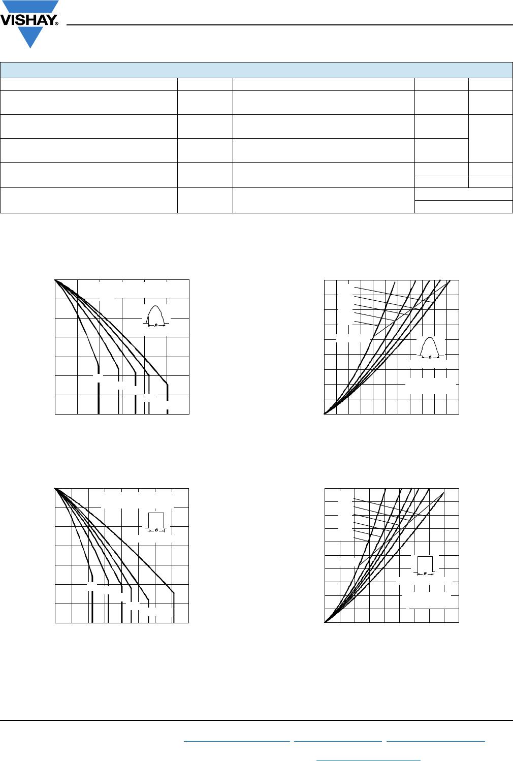
Fig. 1 - Current Rating Characteristics
Fig. 2 - Current Rating Characteristics
Fig. 3 - On-State Power Loss Characteristics
Fig. 4 - On-State Power Loss Characteristics
THERMAL - MECHANICAL SPECIFICATIONS
PARAMETER SYMBOL TEST CONDITIONS VALUES UNITS
Maximum junction and storage
temperature range
T
J
, T
Stg
-40 to +125 °C
Maximum thermal resistance,
junction to case
R
thJC
DC operation 1.3
°C/W
Typical thermal resistance,
junction to ambient
R
thJA
PCB mount
(1)
40
Approximate weight
2g
0.07 oz.
Marking device Case style D
2
PAK (TO-263AB)
16TTS08S
16TTS12S
90
95
100
105
110
115
120
125
024681012
30°
60°
90°
12
18
Conduction Angle
Average On-state Current (A)
Maximum Allowable Case Temperature (°C)
16TTS.. Series
R (DC) = 1.3 °C/W
thJC
90
95
100
105
110
115
120
125
0246810121416
DC
30°
60°
90°
120°
180°
Maximum Allowable Case Temperature (°C)
Conduction Period
Average On-state Current (A)
16TTS.. Series
R (DC) = 1.3 °C/W
thJC
0
2
4
6
8
10
12
14
16
18
01234567891011
RMS Limit
18
12
90°
60°
30°
Cond uction An gle
Average On-state Current (A)
Maximum Average On-state Power Loss (W)
16TTS.. Series
T = 125°C
J
0
5
10
15
20
25
024681012141618
DC
180°
120°
90°
60°
30°
RMS Limit
Conduction Period
Average On-state Current (A)
Max imum Average On-state Power Loss (W)
16TTS.. Series
T = 125°C
J

VS-16TTS08STRR-M3

Mfr. #:
Manufacturer:
Vishay Semiconductors
Description:
SCRs New Input Thyristor - D2PAK-e3
Lifecycle:
New from this manufacturer.
Delivery:
DHL FedEx Ups TNT EMS
Payment:
T/T Paypal Visa MoneyGram Western Union