© Semiconductor Components Industries, LLC, 2016
July, 2016 − Rev. 9
1 Publication Order Number:
MC10E137/D
MC10E137, MC100E137
5 V ECL 8‐Bit Ripple Counter
Description
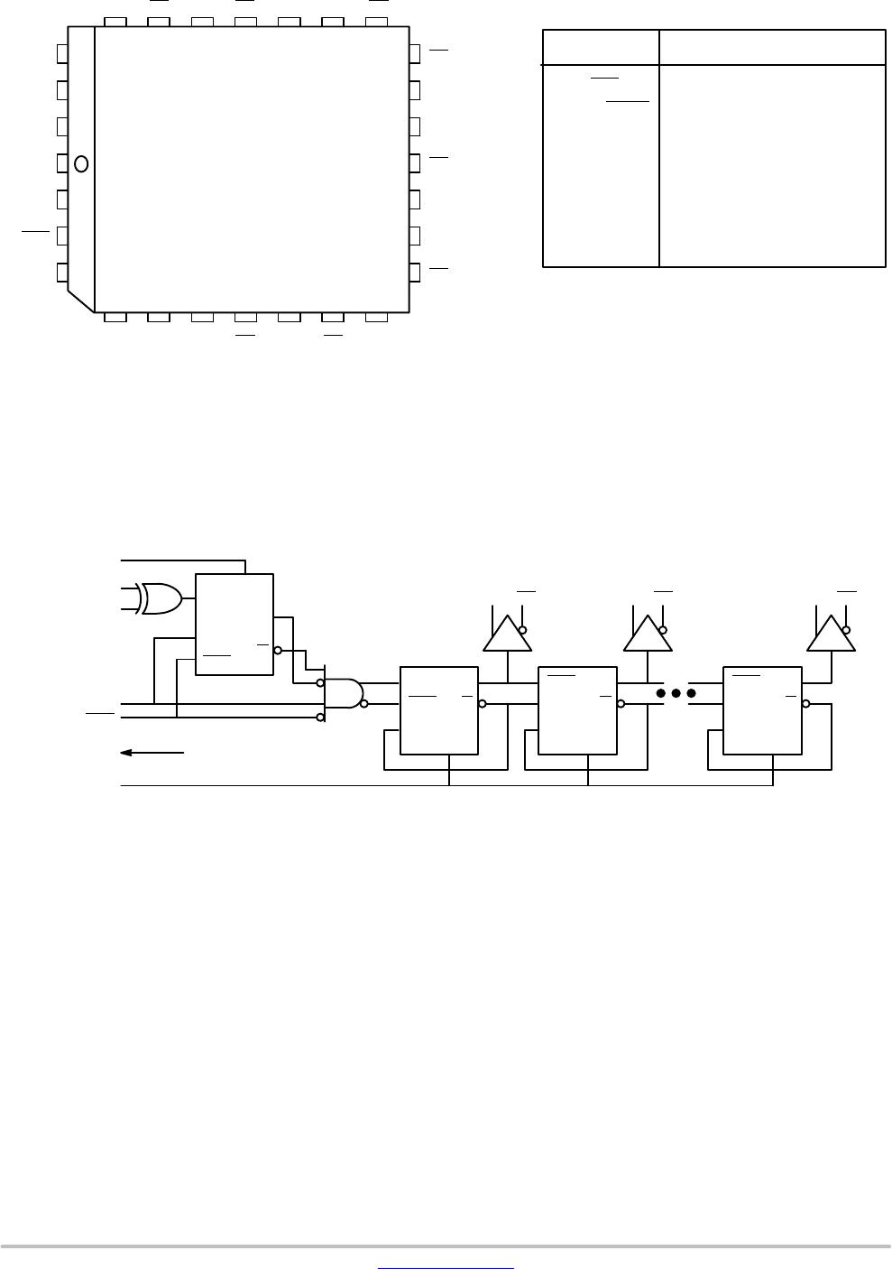
The MC10E/100E137 is a very high speed binary ripple counter. The
two least significant bits were designed with very fast edge rates while
the more significant bits maintain standard ECLinPS™ output edge
rates. This allows the counter to operate at very high frequencies while
maintaining a moderate power dissipation level.
The device is ideally suited for multiple frequency clock generation
as well as a counter in a high performance ATE time measurement
board.
Both asynchronous and synchronous enables are available to
maximize the device’s flexibility for various applications. The
asynchronous enable input, A_Start, when asserted enables the counter
while overriding any synchronous enable signals. The E137 features
XORed enable inputs, EN1 and EN2, which are synchronous to the
CLK input. When only one synchronous enable is asserted the counter
becomes disabled on the next CLK transition; all outputs remain in the
previous state poised for the other synchronous enable or A_Start to be
asserted to re-enable the counter. Asserting both synchronous enables
causes the counter to become enabled on the next transition of the CLK.
If EN1 (or EN2) and CLK edges are coincident, sufficient delay has
been inserted in the CLK path (to compensate for the XOR gate delay
and the internal D-flip flop setup time) to insure that the synchronous
enable signal is clocked correctly, hence, the counter is disabled.
All input pins left open will be pulled LOW via an input pulldown
resistor. Therefore, do not leave the differential CLK inputs open.
Doing so causes the current source transistor of the input clock gate to
become saturated, thus upsetting the internal bias regulators and
jeopardizing the stability of the device.
The asynchronous Master Reset resets the counter to an all zero state
upon assertion.
The V
BB
pin, an internally generated voltage supply, is available to
this device only. For single-ended input conditions, the unused
differential input is connected to V
BB
as a switching reference voltage.
V
BB
may also rebias AC coupled inputs. When used, decouple V
BB
and
V
CC
via a 0.01 mF capacitor and limit current sourcing or sinking to
0.5 mA. When not used, V
BB
should be left open.
The 100 Series contains temperature compensation.
Features
• Differential Clock Input and Data Output Pins
• V
BB
Output for Single-Ended Use
• Synchronous and Asynchronous Enable Pins
• Asynchronous Master Reset
• PECL Mode Operating Range:
♦ V
CC
= 4.2 V to 5.7 V with V
EE
= 0 V
• NECL Mode Operating Range:
♦ V
CC
= 0 V with V
EE
= −4.2 V to −5.7 V
• Internal Input 50 kW Pull-down Resistors
• Transistor Count = 330 devices
• ESD Protection:
♦ Human Body Model: > 2 kV
♦ Machine Model: > 200 V
• Meets or Exceeds JEDEC Spec EIA/JESD78 IC
Latchup Test
• Moisture Sensitivity Level: 3 (Pb-Free)
♦ For Additional Information, see Application Note
AND8003/D
• Flammability Rating: UL 94 V−0 @ 0.125 in,
Oxygen Index: 28 to 34
• These Devices are Pb-Free, Halogen Free and are
RoHS Compliant
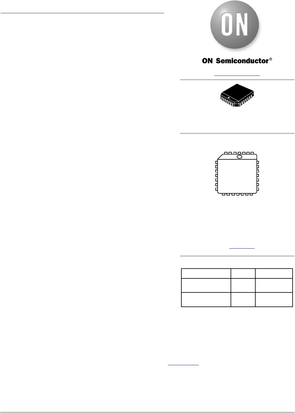
MARKING DIAGRAM*
xxx = 10 or 100
A = Assembly Location
WL = Wafer Lot
YY = Year
WW = Work Week
G = Pb-Free Package
PLCC−28
FN SUFFIX
CASE 776−02
MCxxxE137FNG
AWLYYWW
1
www.onsemi.com
*For additional marking information, refer to
Application Note AND8002/D
.
ORDERING INFORMATION
Device Package Shipping
†
MC10E137FNG PLCC−28
(Pb-Free)
37 Units/Tube
MC100E137FNG PLCC−28
(Pb-Free)
37 Units/Tube