4
AT49F1024/1025
0765I05/01
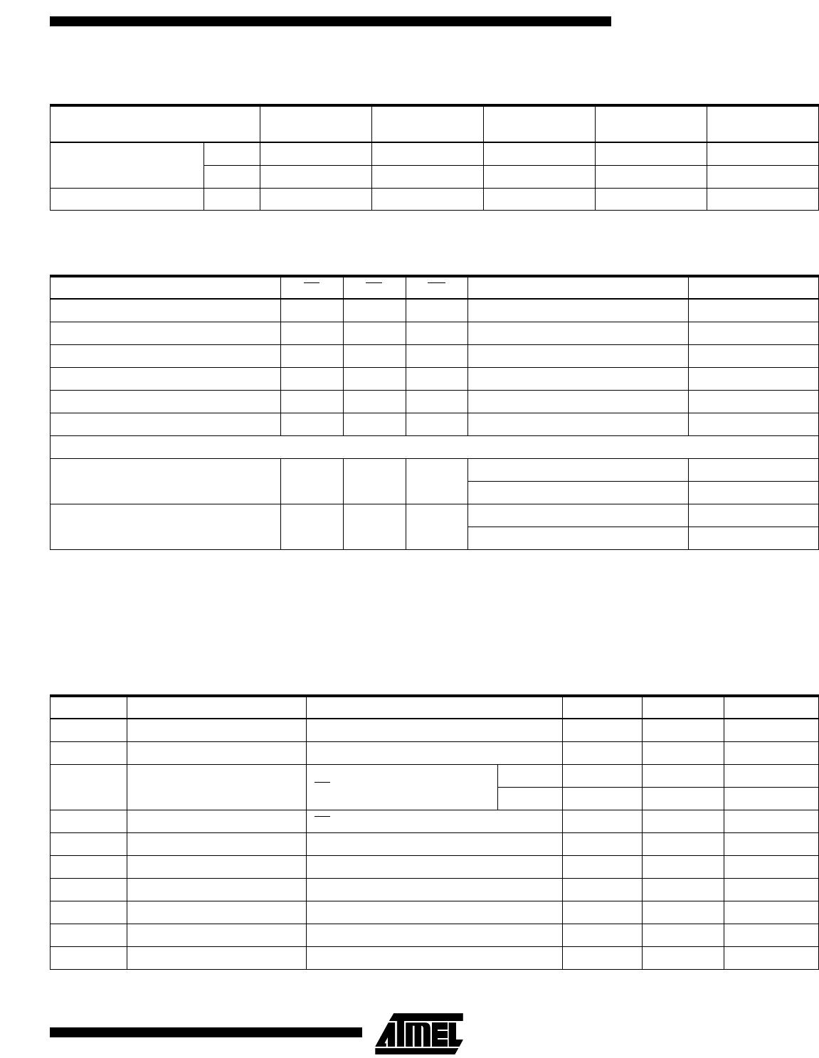
Notes: 1. The DATA FORMAT in each bus cycle is as follows: I/O15 - I/O8 (Dont Care); I/O7 - I/O0 (Hex).
The ADDRESS FORMAT in each bus cycle is as follows: A15 - A0 (Hex); A15 (Dont Care).
2. The 8K word boot sector has the address range 00000H to 1FFFH.
3. Either one of the Product ID Exit commands can be used.
Command Definition (in Hex)
Command
Sequence
Bus
Cycles
1st Bus
Cycle
2nd Bus
Cycle
3rd Bus
Cycle
4th Bus
Cycle
5th Bus
Cycle
6th Bus
Cycle
Addr Data Addr Data Addr Data Addr Data Addr Data Addr Data
Read 1 Addr D
OUT
Chip Erase 6 5555 AA 2AAA 55 5555 80 5555 AA 2AAA 55 5555 10
Main Memory Erase 6 5555 AA 2AAA 55 5555 80 5555 AA 2AAA 55 5555 30
Word Program 4 5555 AA 2AAA 55 5555 A0 Addr D
IN
Boot Block Lockout
(2)
6 5555 AA 2AAA 55 5555 80 5555 AA 2AAA 55 5555 40
Product ID Entry 3 5555 AA 2AAA 55 5555 90
Product ID Exit
(3)
3 5555 AA 2AAA 55 5555 F0
Product ID Exit
(3)
1xxxxF0
Absolute Maximum Ratings*
Temperature under Bias ................................ -55°C to +125°C
*NOTICE: Stresses beyond those listed under Absolute
Maximum Ratings may cause permanent dam-
age to the device. This is a stress rating only and
functional operation of the device at these or any
other conditions beyond those indicated in the
operational sections of this specification is not
implied. Exposure to absolute maximum rating
conditions for extended periods may affect device
reliability.
Storage Temperature ..................................... -65°C to +150°C
All Input Voltages
(including NC Pins)
with Respect to Ground ...................................-0.6V to +6.25V
All Output Voltages
with Respect to Ground .............................-0.6V to V
CC
+ 0.6V
Voltage on OE
with Respect to Ground ...................................-0.6V to +13.5V
5
AT49F1024/1025
0765I05/01
Notes: 1. X can be V
IL
or V
IH
.
2. Refer to AC programming waveforms.
3. V
H
= 12.0V ± 0.5V.
4. Manufacturer Code: 001FH, Device Code: 0087H.
5. See details under Software Product Identification Entry/Exit on page 11.
Note: 1. In the erase mode, I
CC
is 90 mA.
DC and AC Operating Range
AT49F1024-35
AT49F1025-35
AT49F1024-45
AT49F1025-45 AT49F1024-50
AT49F1024-55
AT49F1025-55
AT49F1024-70
AT49F1025-70
Operating
Temperature (Case)
Com. 0°C - 70°C0°C - 70°C0°C - 70°C0°C - 70°C0°C - 70°C
Ind. -40°C - 85°C-40°C - 85°C
V
CC
Power Supply 5V ± 10% 5V ± 10% 5V ± 10% 5V ± 10% 5V ± 10%
Operating Modes
Mode CE OE WE Ai I/O
Read V
IL
V
IL
V
IH
Ai D
OUT
Program
(2)
V
IL
V
IH
V
IL
Ai D
IN
Standby/Write Inhibit V
IH
X
(1)
X X High-Z
Program Inhibit X X V
IH
Program Inhibit X V
IL
X
Output Disable X V
IH
X High-Z
Product Identification
Hardware V
IL
V
IL
V
IH
A1 - A15 = V
IL
, A9 = V
H
(3)
, A0 = V
IL
Manufacturer Code
(4)
A1 - A15 = V
IL
, A9 = V
H
(3)
, A0 = V
IH
Device Code
(4)
Software
(5)
A0 = V
IL
, A1 - A15 = V
IL
Manufacturer Code
(4)
A0 = V
IH
, A1 - A15 = V
IL
Device Code
(4)
DC Characteristics
Symbol Parameter Condition Min Max Units
I
LI
Input Load Current V
IN
= 0V to V
CC
10.0 µA
I
LO
Output Leakage Current V
I/O
= 0V to V
CC
10.0 µA
I
SB1
V
CC
Standby Current CMOS CE = V
CC
- 0.3V to V
CC
Com. 100.0 µA
Ind. 300.0 µA
I
SB2
V
CC
Standby Current TTL CE = 2.0V to V
CC
3.0 mA
I
CC
(1)
V
CC
Active Current f = 5 MHz; I
OUT
= 0 mA 50.0 mA
V
IL
Input Low Voltage 0.8 V
V
IH
Input High Voltage 2.0 V
V
OL
Output Low Voltage I
OL
= 2.1 mA 0.45 V
V
OH1
Output High Voltage I
OH
= -400 µA 2.4 V
V
OH2
Output High Voltage CMOS I
OH
= -100 µA; V
CC
= 4.5V 4.2 V
6
AT49F1024/1025
0765I05/01
AC Read Waveforms
(1)(2)(3)(4)
Notes: 1. CE may be delayed up to t
ACC
- t
CE
after the address transition without impact on t
ACC
.
2. OE
may be delayed up to t
CE
- t
OE
after the falling edge of CE without impact on t
CE
or by t
ACC
- t
OE
after an address change
without impact on t
ACC
.
3. t
DF
is specified from OE or CE, whichever occurs first (C
L
= 5 pF).
4. This parameter is characterized and is not 100% tested.
AC Read Characteristics
Symbol Parameter
AT49F1024-35
AT49F1025-35
AT49F1024-45
AT49F1025-45 AT49F1024-50
AT49F1024-55
AT49F1025-55
AT49F1024-70
AT49F1025-70
UnitsMin Max Min Max Min Max Min Max Min Max
t
ACC
Address to Output Delay 35 45 50 55 70 ns
t
CE
(1)
CE to Output Delay 3545505570ns
t
OE
(2)
OE to Output Delay025030303035ns
t
DF
(3)(4)
CE or OE to Output Float 0 25 0 25 25 0 25 0 25 ns
t
OH
Output Hold from OE,
CE
or Address,
whichever occurred first
00000ns

AT49F1024-55VI

Mfr. #:
Manufacturer:
Description:
IC FLASH 1M PARALLEL 40VSOP
Lifecycle:
New from this manufacturer.
Delivery:
DHL FedEx Ups TNT EMS
Payment:
T/T Paypal Visa MoneyGram Western Union