IDT
®
Two Output Differential Buffer for PCIe Gen1 & Gen2 852 REV Q 08/27/13
ICS9DB102
Two Output Differential Buffer for PCIe Gen1 & Gen2
2
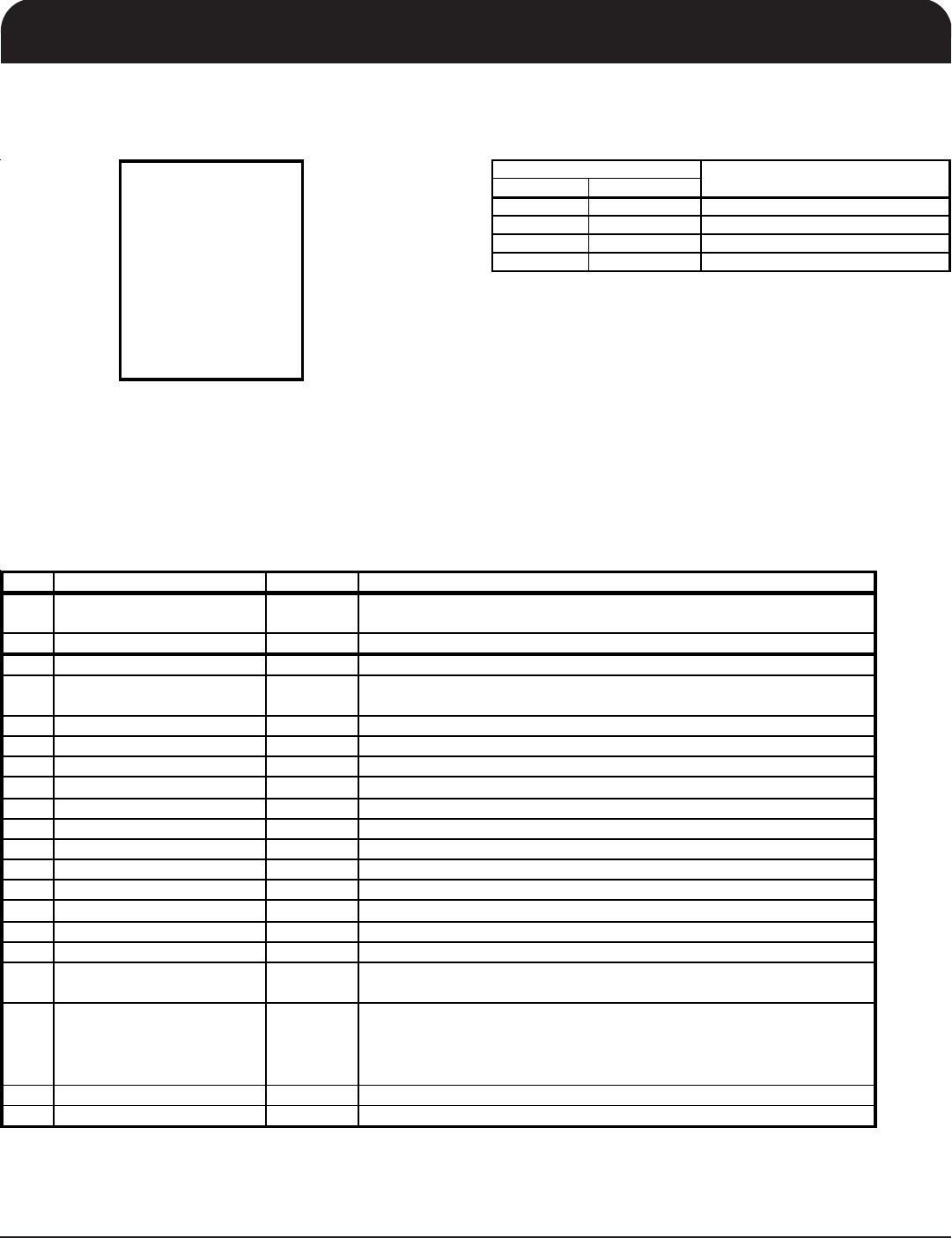
Pin Configuration
20-pin SSOP & TSSOP
VDD GND
5,9,12,16 6,15
PCI Ex
ress Out
uts
96
SMBUS
20 19 IREF
20 19 Analog VDD & GND for PLL core
Description
Pin Number
Power Groups
Pin Description
PLL_BW 1 20 VDDA
CLK_INT 2 19 GNDA
C LK_ INC 3 18 IREF
vCL KREQ0 # 4 17 vC LKREQ1#
VDD 5 16 VDD
GND 6 15 GND
PCIEXT0 7 14 PCIEXT1
PCIEXC0 8 13 PCIEXC1
VDD 9 12 VDD
SMBDAT
10 11 SMBCLK
ICS9DB102
Note:
Pins preceeded by ' v ' have internal
120K ohm pull down resistors
PIN # PIN NA ME PIN TYPE DESCRIPTION
1PLL_BW IN
3.3V inp ut for selectin g PLL Band Width
0 = low, 1= hi
h
2 CLK_INT IN True In
ut for differential reference clock.
3 CLK_INC IN Complementary Input for differential reference clock.
4 v CL KR EQ0 # IN
Output enabl e for PCI Expres s output pai r 0.
0 = enabled, 1 =disabled
5 VDD PWR Power su
l
, nominal 3.3V
GND PWR Ground
in.
PCIEXT0 OUT True clock of differential PCI_Ex
ress
air.
8 PCIEXC0 OUT Complementary clock of differential PCI_Express pair.
9 VDD PWR Power supply, nominal 3.3V
10 SMBD AT I/O D ata pin o f SM BU S c ircuitr y, 5V tol erant
11 SMBC LK IN Clock
in of SMBUS circuitr
, 5V tolerant
12 VDD PWR Power su
l
, nominal 3.3V
13 PC IEXC1 OU T C om
lementar
clock of differential PCI_Ex
ress
air.
14 PCIEXT1 OUT True clock of differential PCI_Express pair.
15 GND PWR Ground pin.
16 VDD PWR Power supply, nominal 3.3V
17 v CLKR EQ1# IN
Output enabl e for PCI Expres s output pai r 1.
0 = enabled, 1 =disabled
18 IREF OU T
This pin establi shes the r efe rence for the differ ential curr ent-m ode
output pairs. It requires a fixed precision resistor to ground. 475ohm is
the standard value for 100ohm differential impedance. Other
im
edanc es re
uire different values. See data sheet.
19 GNDA PWR Ground pin for the PLL core.
20 VDDA PWR 3.3V power for the PLL core.
Pins preceeded by ' v ' have internal 120K ohm pull down resistors
Note:

