MAX7401/MAX7405
8th-Order, Lowpass, Bessel,
Switched-Capacitor Filters
_______________________________________________________________________________________ 7
NAME FUNCTION
1 COM
Common Input. Biased internally at mid-supply. Bypass externally to GND with a 0.1µF capacitor. To over-
ride internal biasing, drive with an external supply.
2 IN Filter Input
PIN
3 GND Ground
4 V
DD
Positive Supply Input: +5V for MAX7401, +3V for MAX7405
8 CLK
Clock Input. To override the internal oscillator, connect to an external clock; otherwise, connect an external
capacitor (C
OSC
) from CLK to GND to set the internal oscillator frequency.
7
SHDN
Shutdown Input. Drive low to enable shutdown mode; drive high or connect to V
DD
for normal operation.
6 OS
Offset Adjust Input. To adjust output offset, bias OS externally. Connect OS to COM if no offset adjustment is
needed. Refer to
Offset and Common-Mode Input Adjustment
section.
5 OUT Filter Output
Pin Description
_______________Detailed Description
The MAX7401/MAX7405 Bessel filters provide low over-
shoot and fast settling responses. Both parts operate
with a 100:1 clock-to-corner frequency ratio and a 5kHz
maximum corner frequency.
Lowpass Bessel filters such as the MAX7401/MAX7405
delay all frequency components equally, preserving the
shape of step inputs (subject to the attenuation of the
higher frequencies). Bessel filters settle quickly—an
important characteristic in applications that use a multi-
plexer (mux) to select an input signal for an analog-to-
digital converter (ADC). An anti-aliasing filter placed
between the mux and the ADC must settle quickly after
a new channel is selected.
Figure 1 shows the difference between Bessel and
Butterworth filters when a 1kHz square wave is applied
to the filter input. With the filter cutoff frequencies set at
5kHz, trace B shows the Bessel filter response and
trace C shows the Butterworth filter response.
Background Information
Most switched-capacitor filters (SCFs) are designed with
biquadratic sections. Each section implements two filter-
ing poles, and the sections are cascaded to produce
higher order filters. The advantage to this approach is
ease of design. However, this type of design is highly
sensitive to component variations if any section’s Q is
high. An alternative approach is to emulate a passive net-
work using switched-capacitor integrators with summing
and scaling. Figure 2 shows a basic 8th-order ladder filter
structure.
A
2V/div
2V/div
2V/div
C
A: 1kHz INPUT SIGNAL
B: BESSEL FILTER RESPONSE; f
C
= 5kHz
C: BUTTERWORTH FILTER RESPONSE; f
C
= 5kHz
B
200µs/div
Figure 1. Bessel vs. Butterworth Filter Response
L3
L5 L7
C8
R2
C4C2
V
IN
+
-
V
0
L1
R1
C6
Figure 2. 8th-Order Ladder Filter Network
MAX7401/MAX7405
8th-Order, Lowpass, Bessel,
Switched-Capacitor Filters
8 _______________________________________________________________________________________
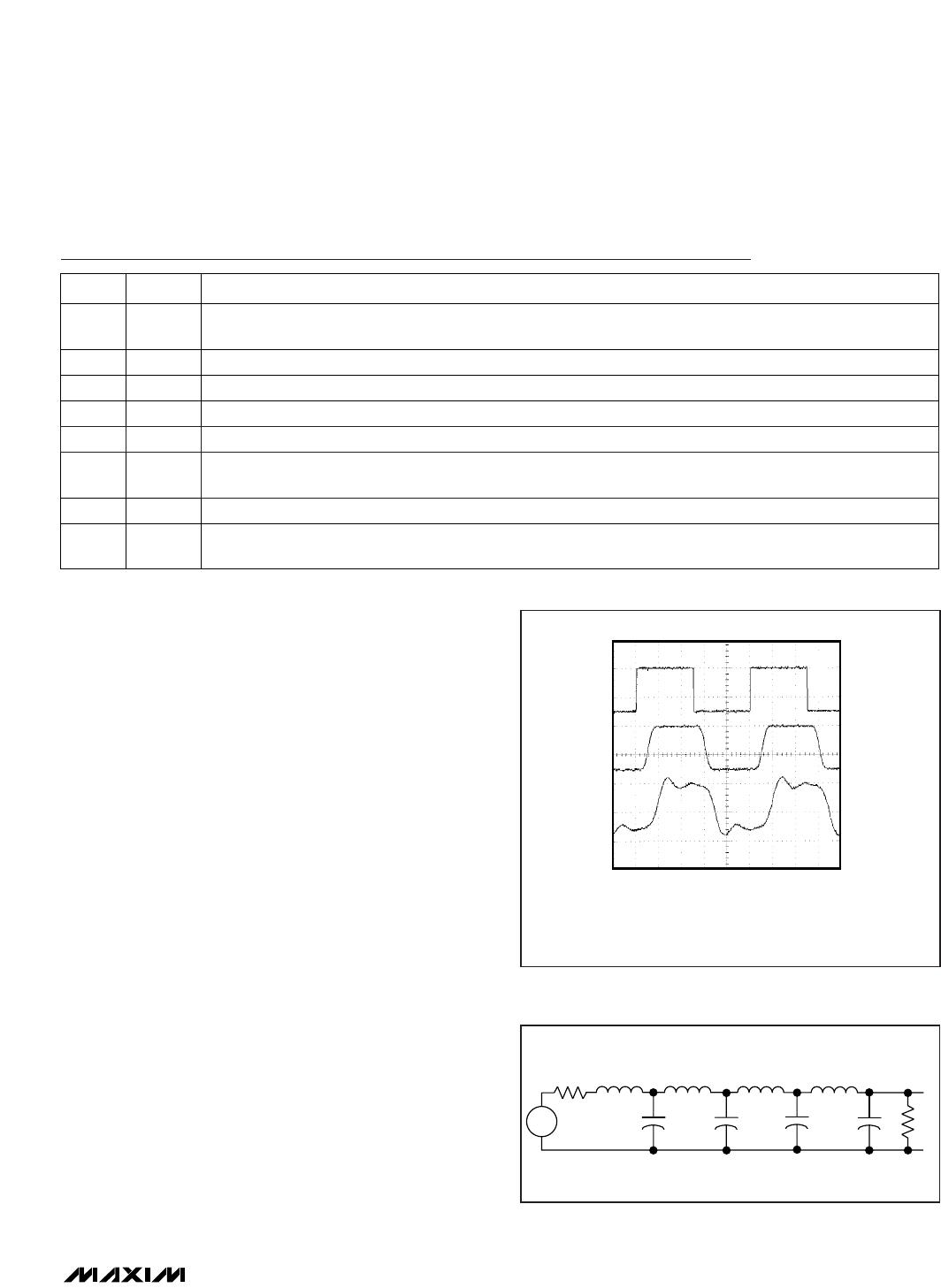
A switched-capacitor filter such as the MAX7401/
MAX7405 emulates a passive ladder filter. The filter’s
component sensitivity is low when compared to a cas-
caded biquad design because each component affects
the entire filter shape, not just one pole-zero pair. In other
words, a mismatched component in a biquad design will
have a concentrated error on its respective poles, while
the same mismatch in a ladder filter design results in an
error distributed over all poles.
Clock Signal
External Clock
The MAX7401/MAX7405 family of SCFs is designed for
use with external clocks that have a 40% to 60% duty
cycle. When using an external clock with these devices,
drive CLK with a CMOS gate powered from 0 to V
DD
.
Varying the rate of the external clock adjusts the corner
frequency of the filter as follows:
f
C
= f
CLK
/ 100
Internal Clock
When using the internal oscillator, connect a capacitor
(C
OSC
) between CLK and ground. The value of the
capacitor determines the oscillator frequency as follows:
where K = 38 for MAX7401 and K = 34 for MAX7405.
Minimize the stray capacitance at CLK so that it does
not affect the internal oscillator frequency. Vary the rate
of the internal oscillator to adjust the filter’s corner fre-
quency by a 100:1 clock-to-corner frequency ratio. For
example, an internal oscillator frequency of 100kHz
produces a nominal corner frequency of 1kHz.
Input Impedance vs. Clock Frequencies
The MAX7401/MAX7405’s input impedance is effectively
that of a switched-capacitor resistor and is inversely pro-
portional to frequency. The input impedance values
determined below represent the average input imped-
ance since the input current is not continuous. As a rule,
use a driver with an output impedance less than 10% of
the filter’s input impedance. Estimate the input imped-
ance of the filter using the following formula:
where f
CLK
= clock frequency and C
IN
= 3.37pF.
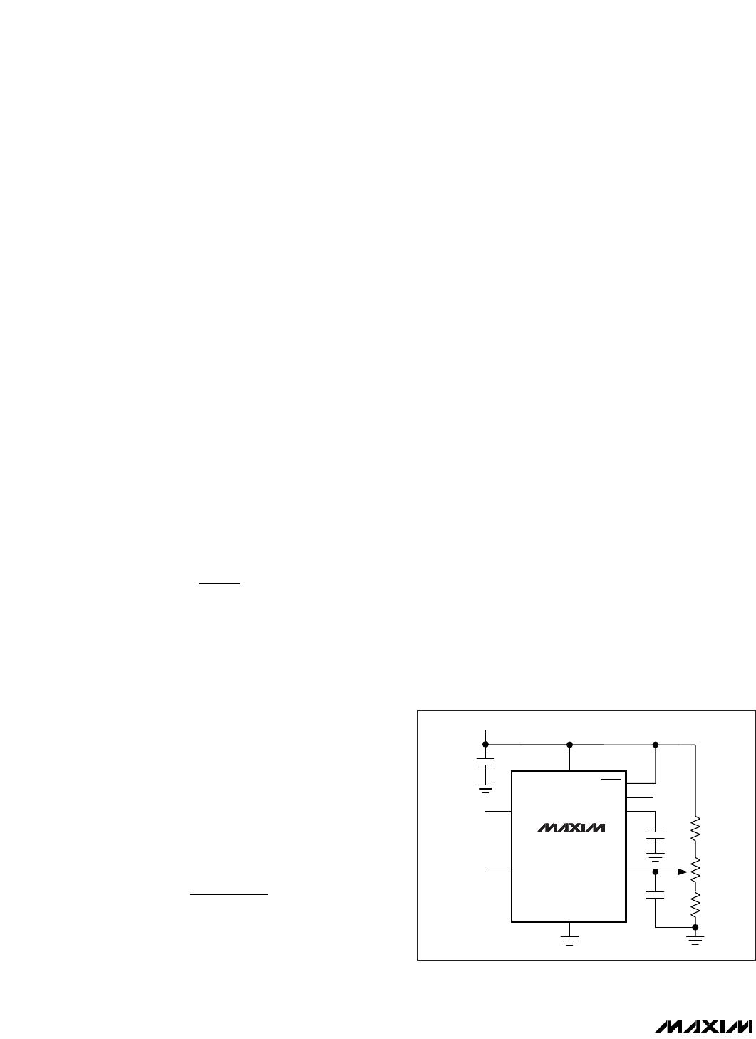
Low-Power Shutdown Mode
These devices feature a shutdown mode that is activat-
ed by driving SHDN low. In shutdown mode, the filter’s
supply current reduces to 0.2µA (typ) and its output
becomes high impedance. For normal operation, drive
SHDN high or connect to V
DD
.
___________Applications Information
Offset and Common-Mode
Input Adjustment
The voltage at COM sets the common-mode input volt-
age and is biased at mid-supply with an internal resistor-
divider. Bypass COM with a 0.1µF capacitor and
connect OS to COM. For applications requiring offset
adjustment or DC level shifting, apply an external bias
voltage through a resistor-divider network to OS, as
shown in Figure 3. (Note: Do not leave OS unconnect-
ed.) The output voltage is represented by this equation:
V
OUT
= (V
IN
- V
COM
) + V
OS
with V
COM
= V
DD
/ 2 (typical), and where (V
IN
- V
COM
) is
lowpass filtered by the SCF, and V
OS
is added at the
output stage. See the
Electrical Characteristics
for the
voltage range of COM and OS. Changing the voltage on
COM or OS significantly from mid-supply reduces the fil-
ter’s dynamic range.
Power Supplies
The MAX7401 operates from a single +5V supply, and
the MAX7405 operates from a single +3V supply.
Bypass V
DD
to GND with a 0.1µF capacitor. If dual sup-
plies are required (±2.5V for MAX7401, ±1.5V for
MAX7405), connect COM to system ground and connect
Z
1
f C
IN
CLK IN
=
()
f (kHz)
K10
C
; C in pF
OSC
3
OSC
OSC
=
V
DD
V
SUPPLY
IN
CLK
GND
INPUT
OUTPUT
50k
50k
50k
OUT
0.1µF
0.1µF
0.1µF
CLOCK
SHDN
COM
OS
MAX7401
MAX7405
Figure 3. Offset Adjustment Circuit
MAX7401/MAX7405
8th-Order, Lowpass, Bessel,
Switched-Capacitor Filters
_______________________________________________________________________________________ 9
GND to the negative supply. Figure 4 shows an example
of dual-supply operation. Single- and dual-supply perfor-
mance are equivalent. For either single- or dual-supply
operation, drive CLK and SHDN from GND (V- in dual-
supply operation) to V
DD
. For ±5V dual-supply applica-
tions, use the MAX291–MAX297.
Input Signal Amplitude Range
The optimal input signal range is determined by observ-
ing the voltage level at which the total harmonic distor-
tion plus noise (THD+N) is minimized for a given corner
frequency. The
Typical Operating Characteristics
show
graphs of the devices’ THD+N response as the input
signal’s peak-to-peak amplitude is varied. These mea-
surements are made with OS and COM biased at mid-
supply.
Anti-Aliasing and Post-DAC Filtering
When using the MAX7401/MAX7405 for anti-aliasing or
post-DAC filtering, synchronize the DAC and the filter
clocks. If the clocks are not synchronized, beat frequen-
cies may alias into the passband.
The high clock-to-corner frequency ratio (100:1) also
eases the requirements of pre- and post-SCF filtering. At
the input, a lowpass filter prevents the aliasing of fre-
quencies around the clock frequency into the passband.
At the output, a lowpass filter attenuates the clock
feedthrough.
A high clock-to-corner frequency ratio allows a simple
RC lowpass filter, with the cutoff frequency set above
the SCF corner frequency, to provide input anti-aliasing
and reasonable output clock attenuation.
Harmonic Distortion
Harmonic distortion arises from nonlinearities within the
filter. These nonlinearities generate harmonics when a
pure sine wave is applied to the filter input. Table 1 lists
the MAX7401/MAX7405’s typical harmonic-distortion
values with a 10kload at T
A
= +25°C.
V
DD
V+
V-
IN
CLK
GND
INPUT
OUTPUTOUT
0.1µF
CLOCK
*DRIVE SHDN TO V- FOR LOW-POWER SHUTDOWN MODE.
SHDN
COM
OS
0.1µF
MAX7401
MAX7405
*
V+
V-
Figure 4. Dual-Supply Operation
5th
3rd
-92-79
-93-83
500
100
f
CLK
(kHz)
4th
2nd
-92
-90
TYPICAL HARMONIC DISTORTION (dB)
-89
-91
4
5
1
MAX7401
V
IN
(Vp-p)
f
C
(kHz)
FILTER
1000
200
f
IN
(Hz)
Table 1. Typical Harmonic Distortion
TRANSISTOR COUNT: 1116
Chip Information
-88-82
-88-83
500
100
-88
-87
-83
-87
2
5
1
MAX7405
1000
200

MAX7401EPA+

Mfr. #:
Manufacturer:
Maxim Integrated
Description:
Active Filter 8th-Order Lowpass Elliptic Filter
Lifecycle:
New from this manufacturer.
Delivery:
DHL FedEx Ups TNT EMS
Payment:
T/T Paypal Visa MoneyGram Western Union