VS-VSKT230-04PBF

VS-VSK.230..PbF Series
www.vishay.com
Vishay Semiconductors
Revision: 27-Apr-17
4
Document Number: 93053
For technical questions within your region: DiodesAmericas@vishay.com
, DiodesAsia@vishay.com, DiodesEurope@vishay.com
THIS DOCUMENT IS SUBJECT TO CHANGE WITHOUT NOTICE. THE PRODUCTS DESCRIBED HEREIN AND THIS DOCUMENT
ARE SUBJECT TO SPECIFIC DISCLAIMERS, SET FORTH AT www.vishay.com/doc?91000
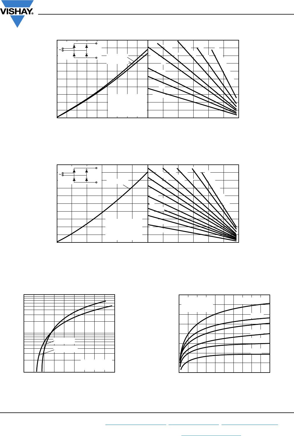
Fig. 3 - On-State Power Loss Characteristics
Fig. 4 - On-State Power Loss Characteristics
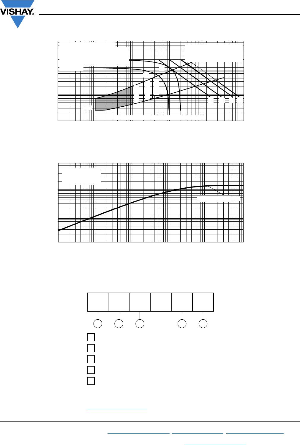
Fig. 5 - Maximum Non-Repetitive Surge Current
Fig. 6 - Maximum Non-Repetitive Surge Current
Fig. 7 - On-State Power Loss Characteristics
Maximum Average On-State
Power Loss (W)
Average On-state Current (A)
250200
150
150
200
250
300
350
100
0
50
100
500
Ø
Conduction Angle
VSK.230..Series
Per Junction
T
J
= 130 °C
180°
120°
90°
60°
30°
RMS limit
Maximum Average On-State
Power Loss (W)
Average On-State Current (A)
250200
150
400350
300
150
200
250
300
350
100
0
50
100
50
0
VSK.230..Series
Per Junction
T
J
= 130 °C
180°
120°
90°
60°
30°
RMS limit
Conduction Period
Ø
DC
Peak Half Sine Wave On-State Current (A)
Number Of Equal Amplitude
Half Cycle Current Pulses (N)
7000
6500
6000
5500
5000
4500
4000
3500
3000
1 10 100
VSK.230..Series
Per Junction
At any rated load condition and with
rated V
RRM
applied following surge
Initial T
J
= 130 °C
at 60 Hz 0.0083 s
at 50 Hz 0.0100 s
Pulse Train Duration (s)
Peak Half Sine Wave On-State Current (A)
7000
7500
6500
6000
5500
5000
4500
4000
3500
3000
0.01 0.1 1
VSK.230..Series
Per Junction
Maximum non repetitive surge current
vs. pulse drain duration.Control of
conduction may not be maintained.
No voltage reapplied
Rated V
RRM
applied
Initial T
J
= 130 °C
Total RMS Output Current (A)
Maximum Total On-State Power Loss (W)
Maximum Allowable Ambient Temperature (°C)
700
600
500
400
300
200
100
200 300 400 500 20 40 60 80 100 120100
0
0
VSK.230..Series
Per Module
T
J
= 130 °C
180°
120°
90°
60°
30°
0.03 K/W
0.06 K/W
0.12 K/W
0.16 K/W
0.2 K/W
0.1 K/W
0.08 K/W
0.25 K/W
R
thSA
= 0.01 K/W - ΔR
0.3 K/W
Conduction Angle
Ø
Ø
VS-VSK.230..PbF Series
www.vishay.com
Vishay Semiconductors
Revision: 27-Apr-17
5
Document Number: 93053
For technical questions within your region: DiodesAmericas@vishay.com
, DiodesAsia@vishay.com, DiodesEurope@vishay.com
THIS DOCUMENT IS SUBJECT TO CHANGE WITHOUT NOTICE. THE PRODUCTS DESCRIBED HEREIN AND THIS DOCUMENT
ARE SUBJECT TO SPECIFIC DISCLAIMERS, SET FORTH AT www.vishay.com/doc?91000
Fig. 8 - On-State Power Loss Characteristics
Fig. 9 - On-State Power Loss Characteristics
Fig. 10 - On-State Voltage Drop Characteristics Fig. 11 - Reverse Recovery Charge Characteristics
Maximum Total Power Loss (W)
Total Output Current (A) Maximum Allowable Ambient Temperature (°C)
20 40 60 80 100 120
1050
900
750
1500
1350
1200
600
450
300
150
0
250 300 350 400 450200150100500
2 x VSK.230..Series
Single phase bridge
connected
T
J
= 130 °C
+
-
180° (Sine)
180° (Rect.)
0.03 K/W
0.06 K/W
0.08 K/W
0.1 K/W
0.16 K/W
0.2 K/W
R
thSA
= 0.01 K/W - Δ
R
1.5 K/W
Maximum Total Power Loss (W)
Total Output Current (A) Maximum Allowable Ambient Temperature (°C)
20 40 60 80 100 120
1400
1200
1000
2000
1800
1600
800
600
400
200
0
300 500400 6002001000
+
-
3 x VSK.230..Series
Three phase bridge
connected
T
J
= 130 °C
120° (Rect.)
0.01 K/W
0.02 K/W
0.04 K/W
0.05 K/W
0.06 K/W
0.03 K/W
R
thSA
= 0.005 K/W - ΔR
0.25 K/W
0.16 K/W
0.12 K/W
0.08 K/W
0.1 K/W
Instantaneous On-State Current (A)
Instantaneous On-State Voltage (V)
VSK.230..Series
Per Junction
T
J
= 25 °C
T
J
= 130 °C
0.5 1 1.5 2 2.5 3 3.5 4 4.5 5
10 000
1000
100
Q
rr -
Typical Reverse Recovery Charge (μC)
200
400
600
800
1000
1200
1400
1600
1800
0 10 20 30 40 50 60 70 80 90 100
VSK.230..Series
Per Junction
T
J
= 130 °C
dI/dt - Rate of Fall of On-State Current (A/μs)
I
TM
= 800 A
500 A
300 A
200 A
100 A
50 A
VS-VSK.230..PbF Series
www.vishay.com
Vishay Semiconductors
Revision: 27-Apr-17
6
Document Number: 93053
For technical questions within your region: DiodesAmericas@vishay.com
, DiodesAsia@vishay.com, DiodesEurope@vishay.com
THIS DOCUMENT IS SUBJECT TO CHANGE WITHOUT NOTICE. THE PRODUCTS DESCRIBED HEREIN AND THIS DOCUMENT
ARE SUBJECT TO SPECIFIC DISCLAIMERS, SET FORTH AT www.vishay.com/doc?91000
Fig. 12 - Gate Characteristics
Fig. 13 - Thermal Impedance Z
thJC
Characteristics
ORDERING INFORMATION TABLE
Note
To order the optional hardware go to www.vishay.com/doc?95172
0.1
1
10
100
0.001 0.01 0.1 1 10 100
VGD
IGD
(b)
(a)
Tj=25 °C
Tj=125 °C
Tj=-40 °C
(2) (3)
Instantaneous Gate Current (A)
Instantaneous Gate Voltage (V)
a) Recommended load line for
b) Recommended load line for
rated di
F
/dt : 20 V, 10 Ω; t
r
< = 1μs
t
r
< = 1 μs
Rectangular gate pulse
< = 30% rated di/dt : 10 V, 20 Ω
(1) PGM = 10 W, tp = 4 ms
(2) PGM = 20 W, tp = 2 ms
(3) PGM = 40 W, tp = 1 ms
(4) PGM = 60 W, tp = 0.66 ms
VSK.230 Series Frequency Limited by PG(AV)
(1) (4)
Device code
KTVS-VS 230 - 20 PbF
1 432 5
- Circuit configuration (see dimensions - link at the end of datasheet)
2
- Current rating
3
- Voltage code x 100 = V
RRM
(see Voltage Ratings table)
4
- • None = standard production
• PbF = lead (Pb)-free
5
- Vishay Semiconductors product
1

VS-VSKT230-04PBF

Mfr. #:
Manufacturer:
Vishay Semiconductors
Description:
SCR Modules 400volt 230amp
Lifecycle:
New from this manufacturer.
Delivery:
DHL FedEx Ups TNT EMS
Payment:
T/T Paypal Visa MoneyGram Western Union