ATV15C130J-HF

This is information on a product in full production.
October 2012 Doc ID 023868 Rev 1 1/7
7
ESDALCL6-2SC6
Very low capacitance and low leakage current ESD protection
Datasheet production data
Features
2 data-line protection
Protects V
BUS
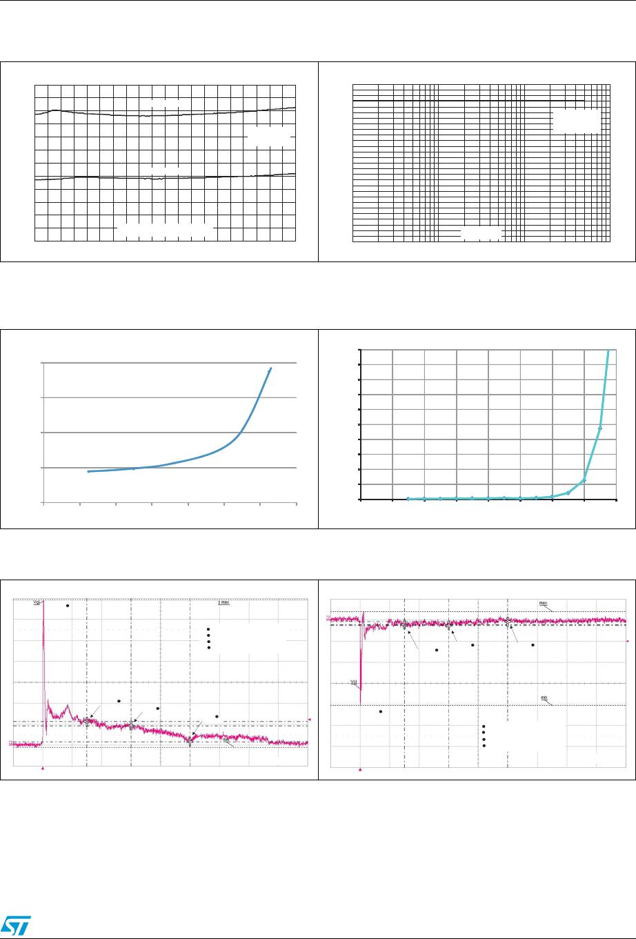
Very low capacitance: 2.5 pF typ.
Very low leakage current:
10 nA at 3 V
1 nA at 1 V
RoHS compliant
Complies with the following standards:
IEC 61000-4-2 level 4 and higher:
30 kV (air discharge)
15 kV (contact discharge)
MIL STD883G-Method 3015-7
25 kV (human body model)
Applications
USB 2.0 ports up to 480 Mb/s (high speed)
Compatible with USB 2.0
Ethernet port: 10/100 Mb/s
SIM card protection
Video line protection
Portable healthcare equipment
Description
The ESDALCL6-2SC6 is a monolithic application
specific device dedicated to ESD protection of
high speed interfaces, such as USB 2.0, ethernet
links and video lines.
The very low line capacitance secures a high level
of signal integrity without compromising in
protecting sensitive chips against the most
stringently characterized ESD strikes.
Its low leakage current makes it suitable for
portable equipment.
Figure 1. Functional diagram (top view)
SOT23-6L
ESDALCL6-2SC6
11
6
2
5
3
4
I/O1 I/O1
GND V
BUS
I/O2 I/O2
www.st.com
Characteristics ESDALCL6-2SC6
2/7 Doc ID 023868 Rev 1
1 Characteristics
Table 1. Absolute ratings
Symbol Parameter Value Unit
V
PP
Peak pulse voltage
IEC 61000-4-2 air discharge
IEC 61000-4-2 contact discharge
MIL STD883G-Method 3015-7
30
15
25
kV
T
stg
Storage temperature range -55 to +150 °C
T
j
Operating junction temperature range -40 to +125 °C
T
L
Lead solder temperature (10 seconds duration) 260 °C
Table 2. Electrical characteristics (T
amb
= 25 °C)
Symbol Parameter Test conditions
Value
Unit
Min. Typ. Max.
V
BR
I
R
= 1 mA 6 V
I
RM
V
RM
= 3 V, V
CC
to GND 10
nA
V
RM
= 1 V, V
CC
to GND 1
V
F
Forward voltage I
F
= 10 mA 1.1 V
V
CL
Clamping voltage
I
PP
= 1 A, 8/20 µs
Any I/O pin to GND
12 V
I
PP
= 5 A, 8/20 µs
Any I/O pin to GND
17 V
C
i/o-GND
Capacitance between I/O and GND V
R
= 1.65 V
2.5 3.5
pF
ΔC
i/o-GND
0.015
C
i/o-i/o
Capacitance between I/O V
R
= 1.65 V
1.2 1.7
pF
ΔC
i/o-i/o
0.04
ESDALCL6-2SC6 Characteristics
Doc ID 023868 Rev 1 3/7
Figure 2. Capacitance versus voltage
(typical values)
Figure 3. Line capacitance versus frequency
(typical values)
0.0
0.5
1.0
1.5
2.0
2.5
3.0
0.0 0.5 1.0 1.5 2.0 2.5 3.0 3.5 4.0 4.5 5.0
C(pF)
F=1MHz
V =30mV
T =25°C
OSC RMS
j
C =I/O-I/O
j
C =I/O-GND
O
Data line voltage (V)
0.0
0.2
0.4
0.6
0.8
1.0
1.2
1.4
1.6
1.8
2.0
2.2
2.4
2.6
2.8
1 10 100 1000
C(pF)
V =30mV
T =25°C
OSC RMS
j
V =0V to 3.3V
LINE
F(MHz)
Figure 4. Leakage current versus junction
temperature (typical values,
V
R
=1V)
Figure 5. Leakage current versus reverse
applied voltage (typical values)
1
10
100
1000
10000
0 20 40 60 80 100 120 140
I
R
(pA)
T (°C)
j
0
200
400
600
800
1000
1200
1400
1600
1800
2000
012345678
I
R
(pA)
V
R
(V)
Figure 6. ESD response to IEC 61000-4-2
(+8 kV contact discharge)
Figure 7. ESD response to IEC 6100-4-2
(-8 kV contact discharge)
20 V/div
138 V
23 V
19 V
1
2
3
3V
4
V : ESD peak voltage
V :clamping voltage at 30 ns
V :clamping voltage at 60 ns
PP
CL
CL
V :clamping voltage at 100 ns
CL
1
2
3
4
20 ns/div
20 V/div
-5 V
-2 V
4
3
20 ns/div
V : ESD peak voltage
V :clamping voltage at 30 ns
V :clamping voltage at 60 ns
PP
CL
CL
V :clamping voltage at 100 ns
CL
1
2
3
4
-81 V
1
-5 V
2

ATV15C130J-HF

Mfr. #:
Manufacturer:
Comchip Technology
Description:
TVS Diodes / ESD Suppressors 1500W 13V UNIDIRECTION AECQ101
Lifecycle:
New from this manufacturer.
Delivery:
DHL FedEx Ups TNT EMS
Payment:
T/T Paypal Visa MoneyGram Western Union