OP297
Rev. G | Page 9 of 16
APPLICATIONS INFORMATION
Extremely low bias current over a wide temperature range
makes the OP297 attractive for use in sample-and-hold
amplifiers, peak detectors, and log amplifiers that must operate
over a wide temperature range. Balancing input resistances is
unnecessary with the OP297. Offset voltage and TCV
OS
are
degraded only minimally by high source resistance, even
when unbalanced.
The input pins of the OP297 are protected against large differen-
tial voltage by back-to-back diodes and current-limiting resistors.
Common-mode voltages at the inputs are not restricted and can
vary over the full range of the supply voltages used.
The OP297 requires very little operating headroom about the
supply rails and is specified for operation with supplies as low as
2 V. Typically, the common-mode range extends to within 1 V
of either rail. The output typically swings to within 1 V of the
rails when using a 10 k load.
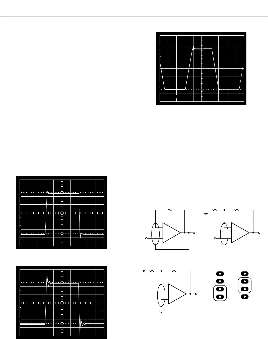
AC PERFORMANCE
The ac characteristics of the OP297 are highly stable over its full
operating temperature range. Unity gain small signal response is
shown in Figure 26. Extremely tolerant of capacitive loading on
the output, the OP297 displays excellent response with 1000 pF
loads (see Figure 27).
10
100
90
0%
10
20mV 5µs
00300-026
Figure 26. Small Signal Transient Response (C
L
= 100 pF, A
VCL
= +1)
5µs
20mV
10
0%
100
90
00300-027
Figure 27. Small Signal Transient Response (C
L
= 1000 pF, A
VCL
= +1)
5µs
20mV
10
0%
100
90
0300-028
Figure 28. Large Signal Transient Response (A
VCL
= +1)
GUARDING AND SHIELDING
To maintain the extremely high input impedances of the OP297,
care is taken in circuit board layout and manufacturing. Board
surfaces must be kept scrupulously clean and free of moisture.
Conformal coating is recommended to provide a humidity
barrier. Even a clean PCB can have 100 pA of leakage currents
between adjacent traces, therefore guard rings should be used
around the inputs. Guard traces operate at a voltage close to that
on the inputs, as shown in Figure 29, to minimize leakage
currents. In noninverting applications, the guard ring should be
connected to the common-mode voltage at the inverting input.
In inverting applications, both inputs remain at ground, so the
guard trace should be grounded. Guard traces should be placed
on both sides of the circuit board.
UNIT
-GAIN FOLLOWER
–
+
1/2
OP297
INVERTING AMPLIFIER
–
+
1/2
OP297
MINI-DIP
BOTTOM VIEW
8
B
1
A
NONINVERTIN
MPLIFIER
–
+
1/2
OP297
00300-029
Figure 29. Guard Ring Layout and Considerations