© Semiconductor Components Industries, LLC, 2013
October, 2013 − Rev. 0
1 Publication Order Number:
MBR10100MFS/D
MBR10100MFS,
NRVB10100MFS
SWITCHMODE
Power Rectifiers
Features
• Low Power Loss / High Efficiency
• New Package Provides Capability of Inspection and Probe After
Board Mounting
• Guardring for Stress Protection
• Low Forward Voltage Drop
• 175°C Operating Junction Temperature
• Wettable Flacks Option Available
• NRVB Prefix for Automotive and Other Applications Requiring
Unique Site and Control Change Requirements; AEC−Q101
Qualified and PPAP Capable
• These are Pb−Free Devices
Mechanical Characteristics:
• Case: Epoxy, Molded
• Epoxy Meets Flammability Rating UL 94−0 @ 0.125 in.
• Lead Finish: 100% Matte Sn (Tin)
• Lead and Mounting Surface Temperature for Soldering Purposes:
260°C Max. for 10 Seconds
• Device Meets MSL 1 Requirements
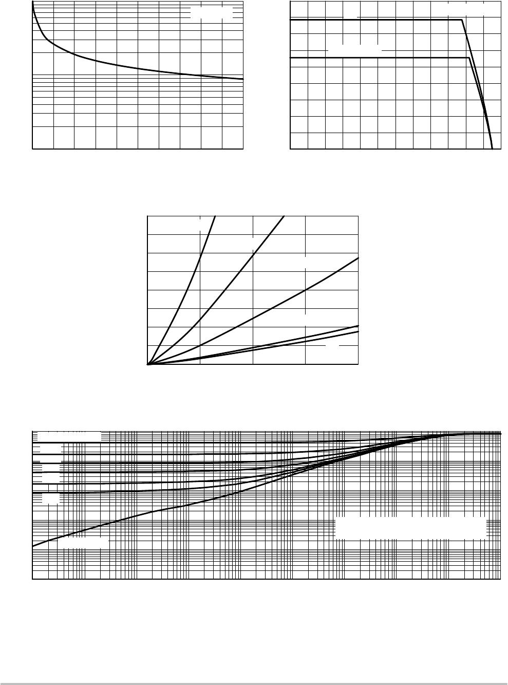
MAXIMUM RATINGS
Rating Symbol Value Unit
Peak Repetitive Reverse Voltage
Working Peak Reverse Voltage
DC Blocking Voltage
V
RRM
V
RWM
V
R
100
V
Average Rectified Forward Current
(Rated V
R
, T
C
= 165°C)
I
F(AV)
10 A
Peak Repetitive Forward Current,
(Rated V
R
, Square Wave,
20 kHz, T
C
= 163°C)
I
FRM
20 A
Non−Repetitive Peak Surge Current
(Surge Applied at Rated Load
Conditions Halfwave, Single
Phase, 60 Hz)
I
FSM
150 A
Storage Temperature Range T
stg
−65 to +175 °C
Operating Junction Temperature T
J
−55 to +175 °C
Unclamped Inductive Switching
Energy (10 mH Inductor,
Non−repetitive)
E
AS
75 mJ
ESD Rating (Human Body Model) 3B
ESD Rating (Machine Model) M4
Stresses exceeding Maximum Ratings may damage the device. Maximum
Ratings are stress ratings only. Functional operation above the Recommended
Operating Conditions is not implied. Extended exposure to stresses above the
Recommended Operating Conditions may affect device reliability.
NOTE: The heat generated must be less than the thermal conductivity from
Junction−to−Ambient: dPD/dTJ < 1/RJA.
Device Package Shipping†
ORDERING INFORMATION
MBR10100MFST1G SO−8 FL
(Pb−Free)
1500 /
Tape & Reel
SCHOTTKY BARRIER
RECTIFIERS
10 AMPERES
100 VOLTS
http://onsemi.com
1,2,3
5,6
SO−8 FLAT LEAD
CASE 488AA
STYLE 2
B10100 = Specific Device Code
A = Assembly Location
Y = Year
W = Work Week
ZZ = Lot Traceability
MARKING
DIAGRAM
B10100
AYWZZ
A
A
A
Not Used
1
†For information on tape and reel specifications,
including part orientation and tape sizes, please
refer to our Tape and Reel Packaging Specification
Brochure, BRD8011/D.
MBR10100MFST3G SO−8 FL
(Pb−Free)
5000 /
Tape & Reel
NRVB10100MFST1G SO−8 FL
(Pb−Free)
1500 /
Tape & Reel
NRVB10100MFST3G SO−8 FL
(Pb−Free)
5000 /
Tape & Reel