ADM6710 Data Sheet
Rev. B | Page 8 of 12
THEORY OF OPERATION
The ADM6710 is a compact, low power supervisory circuit
capable of monitoring up to four voltages in a multisupply
application.
The device includes several factory-set voltage threshold
options for monitoring 1.8 V, 2.5 V, 3.0 V, 3.3 V and 5.0 V
supplies. It also provides up to three adjustable thresholds for
monitoring voltages down to 0.62 V. See the Ordering Guide
section for a list and description of all available options.
The ADM6710Q has three adjustable voltage inputs and is
powered by V
CC
, which is not a monitored voltage. All other
ADM6710 devices are powered by IN
2
, which is a monitored
voltage, and therefore monitors up to four voltages. If a monitored
voltage drops below its associated threshold, the active low reset
output asserts low and remains low while either IN
1
or IN
2
remains
above 1.0 V.
MONITORED
SUPPLIES
MICROPROCESSOR
06626-004
ADM6710
IN
1
IN
2
IN
3
IN
4
GND
RESET
Figure 12. Typical Applications Circuit
INPUT CONFIGURATION
The ADM6710 provides numerous monitor choices with
adjustable reset thresholds. Typically, the threshold voltage at
each adjustable IN
x
input is 0.62 V. To monitor a voltage greater
than 0.62 V, connect a resistor divider network to the circuit as
depicted in Figure 13, where
2
21
62.0
R
RR
VV
INTH
R1
R2
INTH
V
REF
= 0.62V
06626-006
Figure 13. Setting the Adjustable Monitor
The internal comparators each typically have a hysteresis of 0.3%
with respect to the reset threshold. This built-in hysteresis
improves the device’s immunity to ambient noise without
noticeably reducing the threshold accuracy. The ADM6710
is unaffected by short input transients.
The ADM6710 is powered from the monitored IN
2
, or V
CC
in the
case of the ADM6710Q. Monitored inputs are resistant to short
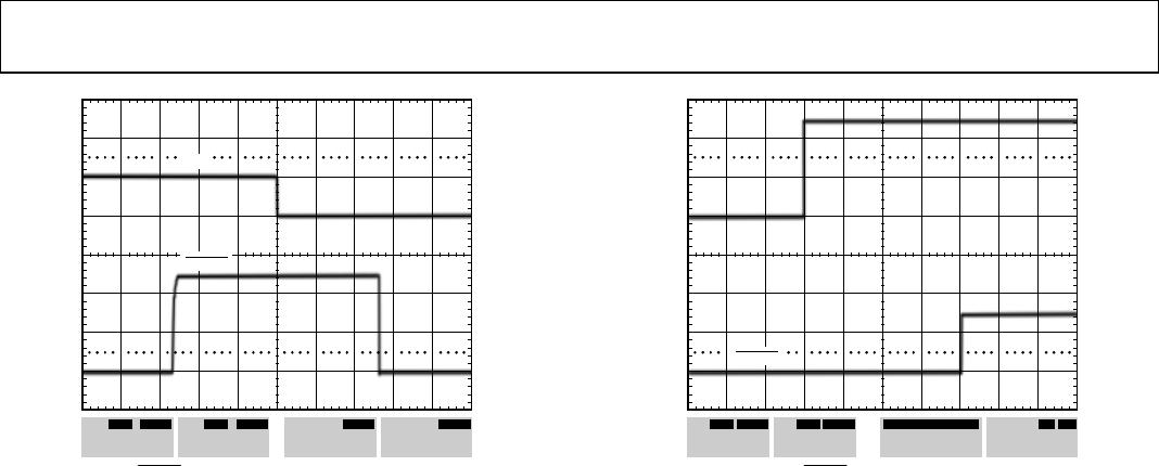
power supply glitches. Figure 7 depicts the ADM6710 glitch
immunity data. To increase noise immunity in noisy applications,
place a 0.1 μF capacitor between the IN
2
input and ground.
Adding capacitance to IN
1
, IN
3
, and IN
4
also improves noise
immunity.
Do not allow unused monitor inputs to float or to be grounded.
Connect these inputs to a supply voltage greater than their specified
threshold voltages. In the case of unused IN
x
adjustable inputs,
limit the bias current by connecting a 1 MΩ series resistor between
the unused input and IN
2
(or V
CC
in the case of the ADM6710Q).
RESET OUTPUT CONFIGURATION
The
RESET
output asserts low if a monitored IN
x
voltage drops
below its voltage threshold. Once all voltages rise above the
selected threshold level, the reset signal remains low for the
reset timeout period (200 ms typical). The reset output is open
drain with a weak internal pull-up to the monitored IN
2
or V
CC
supply, typically 10 μA.
Many applications that interface with other logic devices do not
require an external pull-up resistor. However, if an external
pull-up resistor is required and it is connected to a voltage
ranging from 0 V to 5.5 V, it will overdrive the internal pull-up.
Reverse current flow from the external pull-up voltage to IN
2
is
prevented by the internal circuitry.
ADM6710
RESET
06626-005
RESET
V
CC
5
100kΩ
IN
2
=3.3
Figure 14. Interface with a Different Logic Supply Voltage
ADDITION OF MANUAL RESET
Use the circuit shown in Figure 15 to add manual reset to any of
the ADM6710 adjustable inputs. When the switch is closed, the
analog input shorts to ground and a
RESET
output commences.
The switch must remain open for a minimum of 140 ms for the
RESET
output to deassert.
ADM6710
IN
1
IN
2
IN
3
IN
4
GND
RESET
06626-007
R1
R2
V
IN4
Figure 15. Addition of Manual Reset (IN
4
is an Adjustable Input)