LT6 020/LT6020-1
10
60201fa
For more information www.linear.com/LT6020
Typical perForMance characTerisTics
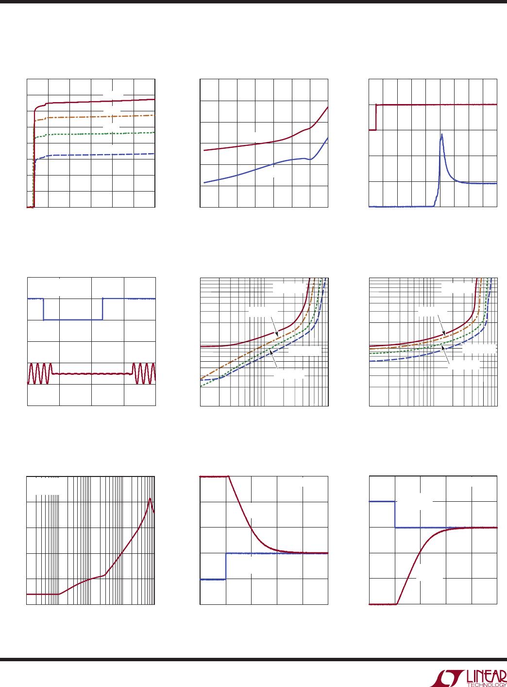
Negative Output Overdrive
Recovery
Positive Output Overdrive
RecoveryCrosstalk vs Frequency
T
A
= 25°C, V
S
= ±15V, R
L
= 100kΩ unless
otherwise specified.
60201 G29
100µs/DIV
0V
INPUT
200mV/DIV
A
V
= –100
OUTPUT
5V/DIV
60201 G30
100µs/DIV
0V
INPUT
200mV/DIV
A
V
= –100
OUTPUT
5V/DIV
FREQUENCY (Hz)
CROSSTALK (dB)
60201 G28
–40
–60
–80
–100
–120
–140
100 1k 1M100k10k
V
DGND
= 0V
V
EN
= 5V
Supply Current vs Supply Voltage
Shutdown Supply Current vs
Temperature
Start-Up Response
Enable/Disable Response
Output Saturation Voltage vs
Sink Current (Output Low)
Output Saturation Voltage vs
Source Current (Output High)
TOTAL SUPPLY VOLTAGE (V)
0
SUPPLY CURRENT/AMPLIFIER (µA)
160
140
120
100
80
60
40
20
0
25 305 20
60201 G22
10 15
125°C
85°C
25°C
–40°C
TEMPERATURE (°C)
–50
SHUTDOWN SUPPLY CURRENT (µA)
3.0
2.5
2.0
1.5
1.0
0.5
0
75 100 125–25 50
60201 G23
0 25
V
S
= 30V
V
S
= 3V
V
EN
5V/DIV
V
OUT
5V/DIV
0V
0V
60201 G24
100µs/DIV
A
V
= 1
V
IN
= 5V
P-P
AT 50kHz
LOAD CURRENT (mA)
OUTPUT LOW SATURATION VOLTAGE (V)
60201 G26
1
0.1
0.01
0.1 1 10
T
A
= 125°C
T
A
= 85°C
T
A
= –40°C
T
A
= 25°C
LOAD CURRENT (mA)
OUTPUT HIGH SATURATION VOLTAGE (V)
60201 G27
1
0.1
0.01
0.1 1 10
T
A
= 125°C
T
A
= 85°C
T
A
= –40°C
T
A
= 25°C
V
EN
5V/DIV
0V
I(V
+
)
200µA/DIV
0µA
60201 G24
20µs/DIV
LT6 020/LT6 020-1
11
60201fa
For more information www.linear.com/LT6020
pin FuncTions
OUT: Amplifier Output.
–IN: Inverting Input of the Amplifier.
+IN: Noninverting Input of the Amplifier.
V
: Negative Power Supply. A bypass capacitor should be
used between supply pins and ground. Additional bypass
capacitance may be used between the power supply pins.
DGND (LT6020-1 Only): Reference for EN Pin. It is normally
tied to ground. DGND must be in the range from V
to V
+
–3V. If grounded, V
+
must be ≥ 3V. The EN pin threshold
is specified with respect to the DGND pin. DGND cannot
be floated.
EN (LT6020-1 Only): Enable Input. This pin must be
connected high, normally to V
+
, for the amplifiers to be
functional. EN is active high with the threshold approxi-
mately two
diodes above DGND. EN cannot be floated.
The
shutdown threshold voltage is specified with respect
to the voltage on the DGND pin.
V
+
: Positive Power Supply. A bypass capacitor should be
used between supply pins and ground. Additional bypass
capacitance may be used between the power supply pins.
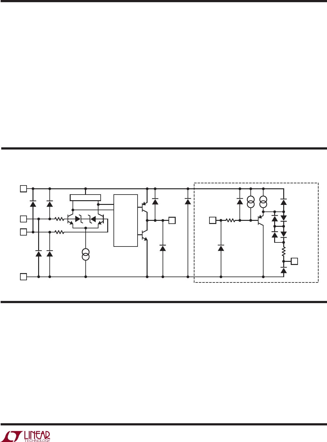
siMpliFieD scheMaTic
60201 BD
+IN
V
+
–IN
5k
5k
OUT
EN
200k
200k
LT6020-1 ONLY
DGND
V
LOAD
CLASS AB
DRIVE
applicaTions inForMaTion
Preserving Low Power Operation
The proprietary circuitry used in the LT6020 provides an
excellent combination of low power, low offset and en
-
hanced slew rate. Normally an amplifier with higher supply
current would be required to achieve this combination of
slew rate and precision. Special care must be taken to
ensure that the low power operation is preserved.
The choice of feedback resistor values impacts several
op-amp parameters as noted in the feedback compo
-
nents section
.
It should also be noted that the output of
the amplifier must drive this network. For example, in a
gain of two with a total feedback resistance of 10kΩ and
an output voltage of 14V, the amplifier’s output will need
to supply 1.4mA of current. This current will ultimately
come from a supply.
LT6 020/LT6020-1
12
60201fa
For more information www.linear.com/LT6020
applicaTions inForMaTion
Figure 1. Settling Time Is Essentially Flat
smaller inputs the LT6020 slew rate approaches the slew
rate more common in traditional micropower amplifiers.
Input Bias Current
The design of the input stage of the LT6020 is more so
-
phisticated than that shown in the Simplified Schematic.
It
uses both NPN and PNP input differential amplifiers to
sense the input differential voltage. As a result the speci
-
fied input bias current can flow in or out of the input pins.
Multiplexer Applications/High Dynamic Input
Impedance
The LT6020 has features which make it desirable for
multiplexer applications, such as the application featured
on the back page of this data sheet. When the channels of
the multiplexer are cycled, the output of the multiplexer
can produce large voltage transitions. Normally, bipolar
amplifiers have back-to-back diodes between the inputs,
which will turn on when the input transient voltage exceeds
0.7V, causing a large transient current to be conducted
from the amplifier output stage back into the input driving
circuitry. The driving circuitry then needs to absorb this
current and settle before the amplifier can settle. The
LT6020 uses 5.5V Zener diodes to protect its inputs which
dramatically increases its
input impedance with input steps
as large as 5V.
Achieving Rail-to-Rail Operation without
Rail-to-Rail Inputs
The LT6020 output is able to swing close to each power
supply rail, but the input stage is limited to operating
between V
+ 1.2V and V
+
– 1.4V. For many inverting
applications and noninverting gain applications, this is
largely inconsequential. Figure 2 shows the basic op amp
configurations, what happens to the op amp inputs and
whether or not the op amp must have rail-to-rail inputs.
The circuit of Figure 3 shows an extreme example of the
inverting case. The input voltage at the 100k resistor can
swing ±13.5V and the LT6020 will output an inverted,
OUTPUT STEP (V
P-P
)
5
SETTLING TIME (µs)
30
25
20
15
10
5
0
20
60201 F01
2510 15
0.0015%
A
V
= 1
0.01%
The supply current of the LT6020 increases with large
differential input voltages. Normally, this does not impact
the low power nature of the LT6020 because the ampli
-
fier is forcing the two inputs to be at the same potential.
Conditions which cause differential input voltage to appear
should be avoided in order to preserve the low power dis
-
sipation of the LT6020. This includes but is not limited
to: operation as a comparator, excessive loading on the
output and overdriving the input.
Enhanced Slew Rate
The LT6020 uses a proprietary input stage which provides
an enhanced slew rate without sacrificing input precision
specs such as input offset voltage, common mode rejection
and noise. The unique input stage of the LT6020 allows the
output to quickly slew to its final value when large signal
input steps are applied. This enhanced slew characteristic
allows the LT6020 to quickly settle the output to 0.0015%
independent of input step size as shown in Figure 1. Typi
-
cal micropower amplifiers cannot process large amplitude
signals with this speed. As shown in the Typical Perfor-
mance cur
ves, when the LT6020 is configured in unity
gain
and a 10V step is applied to the input the output will
slew
at 5V/µs. In this same configuration, a 5V input step
will slew the output at 2.4V/µs. Furthermore, a 0.7V input
step will lower the slew rate to 0.2V/µs. Note that for these
LT6020IMS8#TRPBF

Mfr. #:
Manufacturer:
Analog Devices Inc.
Description:
Precision Amplifiers Dual Micropower Op Amp with Slew Boost
Lifecycle:
New from this manufacturer.
Delivery:
DHL FedEx Ups TNT EMS
Payment:
T/T Paypal Visa MoneyGram Western Union