SMAJ5.0A thru SMAJ188CA
www.vishay.com
Vishay General Semiconductor
Revision: 09-Nov-16
2
Document Number: 88390
For technical questions within your region: DiodesAmericas@vishay.com
, DiodesAsia@vishay.com, DiodesEurope@vishay.com
THIS DOCUMENT IS SUBJECT TO CHANGE WITHOUT NOTICE. THE PRODUCTS DESCRIBED HEREIN AND THIS DOCUMENT
ARE SUBJECT TO SPECIFIC DISCLAIMERS, SET FORTH AT www.vishay.com/doc?91000
Notes
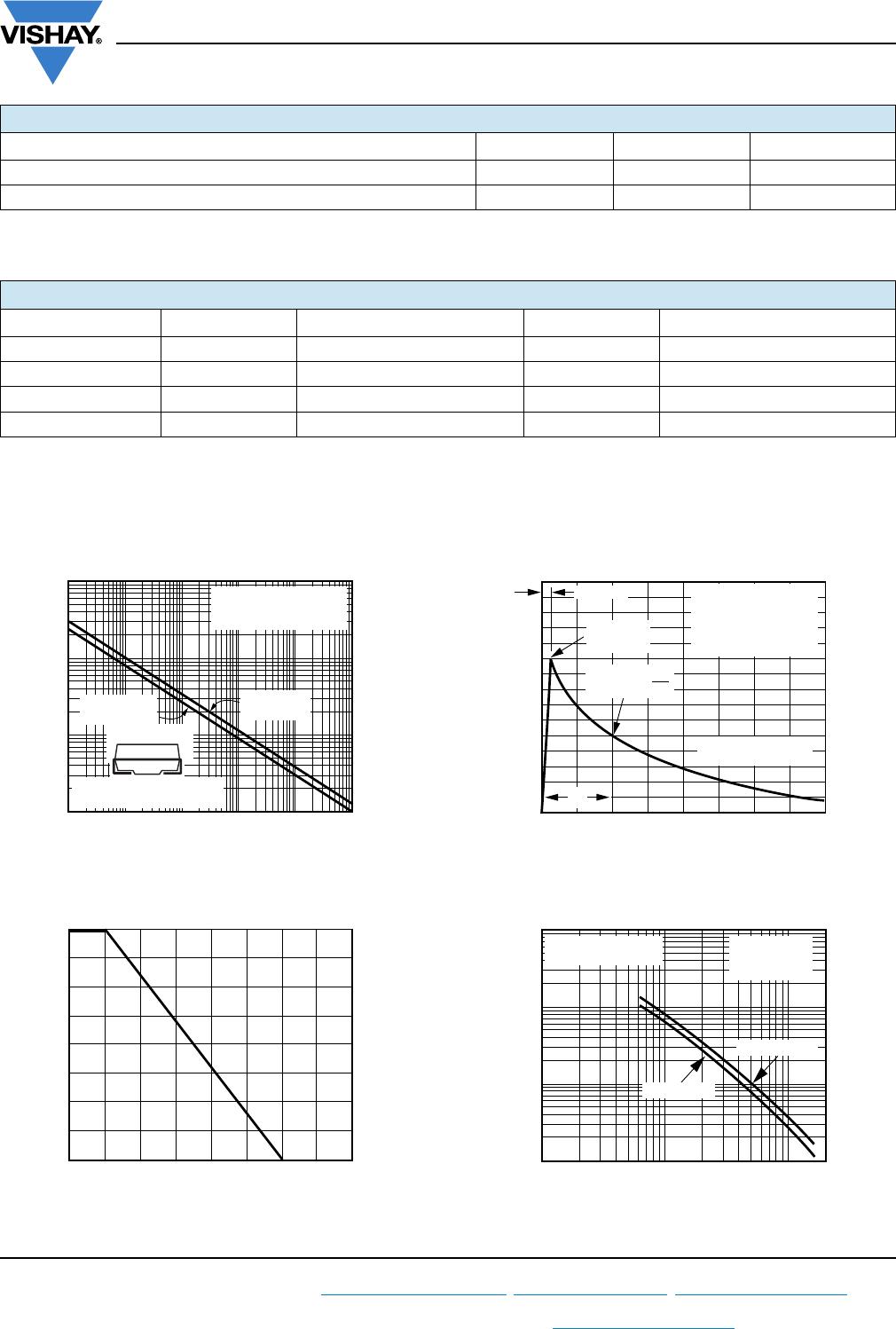
(1)
Pulse test: t
p
50 ms
(2)
Surge current waveform per fig. 3 and derate per fig. 2
(3)
For bi-directional types having V
WM
of 10 V and less, the I
D
limit is doubled
(4)
All terms and symbols are consistent with ANSI/IEEE C62.35
(5)
For the bi-directional SMAJ5.0CA, the maximum V
BR
is 7.25 V
(6)
V
F
= 3.5 V at I
F
= 25 A (uni-directional only)
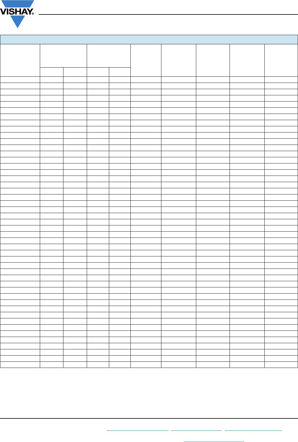
ELECTRICAL CHARACTERISTICS (T
A
= 25 °C unless otherwise noted)
DEVICE TYPE
DEVICE MARKING
CODE
BREAKDOWN
VOLTAGE
V
BR
AT I
T
(1)
(V)
TEST
CURRENT
I
T
(mA)
STAND-OFF
VOLTAGE
V
WM
(V)
MAXIMUM
REVERSE
LEAKAGE
AT V
WM
I
D
(μA)
(3)
MAXIMUM
PEAK PULSE
SURGE
CURRENT
I
PPM
(A)
(2)
MAXIMUM
CLAMPING
VOLTAGE AT
I
PPM
V
C
(V)
UNI BI MIN. MAX.
SMAJ5.0A
(5)
AE WE 6.40 7.07 10 5.0 800 43.5 9.2
SMAJ6.0A AG WG 6.67 7.37 10 6.0 800 38.8 10.3
SMAJ6.5A AK WK 7.22 7.98 10 6.5 500 35.7 11.2
SMAJ7.0A AM WM 7.78 8.60 10 7.0 200 33.3 12.0
SMAJ7.5A AP WP 8.33 9.21 1.0 7.5 100 31.0 12.9
SMAJ8.0A AR WR 8.89 9.83 1.0 8.0 50 29.4 13.6
SMAJ8.5A AT WT 9.44 10.4 1.0 8.5 10 27.8 14.4
SMAJ9.0A AV WV 10.0 11.1 1.0 9.0 5.0 26.0 15.4
SMAJ10A AX WX 11.1 12.3 1.0 10 1.0 23.5 17.0
SMAJ11A AZ WZ 12.2 13.5 1.0 11 1.0 22.0 18.2
SMAJ12A BE XE 13.3 14.7 1.0 12 1.0 20.1 19.9
SMAJ13A BG XG 14.4 15.9 1.0 13 1.0 18.6 21.5
SMAJ14A BK XK 15.6 17.2 1.0 14 1.0 17.2 23.2
SMAJ15A BM XM 16.7 18.5 1.0 15 1.0 16.4 24.4
SMAJ16A BP XP 17.8 19.7 1.0 16 1.0 15.4 26.0
SMAJ17A BR XR 18.9 20.9 1.0 17 1.0 14.5 27.6
SMAJ18A BT XT 20.0 22.1 1.0 18 1.0 13.7 29.2
SMAJ20A BV XV 22.2 24.5 1.0 20 1.0 12.3 32.4
SMAJ22A BX XX 24.4 26.9 1.0 22 1.0 11.3 35.5
SMAJ24A BZ XZ 26.7 29.5 1.0 24 1.0 10.3 38.9
SMAJ26A CE YE 28.9 31.9 1.0 26 1.0 9.5 42.1
SMAJ28A CG YG 31.1 34.4 1.0 28 1.0 8.8 45.4
SMAJ30A CK YK 33.3 36.8 1.0 30 1.0 8.3 48.4
SMAJ33A CM YM 36.7 40.6 1.0 33 1.0 7.5 53.3
SMAJ36A CP YP 40.0 44.2 1.0 36 1.0 6.9 58.1
SMAJ40A CR YR 44.4 49.1 1.0 40 1.0 6.2 64.5
SMAJ43A CT YT 47.8 52.8 1.0 43 1.0 5.8 69.4
SMAJ45A CV YV 50.0 55.3 1.0 45 1.0 5.5 72.7
SMAJ48A CX YX 53.3 58.9 1.0 48 1.0 5.2 77.4
SMAJ51A CZ YZ 56.7 62.7 1.0 51 1.0 4.9 82.4
SMAJ54A RE ZE 60.0 66.3 1.0 54 1.0 4.6 87.1
SMAJ58A RG ZG 64.4 71.2 1.0 58 1.0 4.3 93.6
SMAJ60A RK ZK 66.7 73.7 1.0 60 1.0 4.1 96.8
SMAJ64A RM ZM 71.1 78.6 1.0 64 1.0 3.9 103
SMAJ70A RP ZP 77.8 86.0 1.0 70 1.0 3.5 113
SMAJ75A RR ZR 83.3 92.1 1.0 75 1.0 3.3 121
SMAJ78A RT ZT 86.7 95.8 1.0 78 1.0 3.2 126
SMAJ85A RV ZV 94.4 104 1.0 85 1.0 2.2 137
SMAJ90A RX ZX 100 111 1.0 90 1.0 2.1 146
SMAJ100A RZ ZZ 111 123 1.0 100 1.0 1.9 162
SMAJ110A SE VE 122 135 1.0 110 1.0 1.7 177
SMAJ120A VG VG 133 147 1.0 120 1.0 1.6 193
SMAJ130A VK VK 144 159 1.0 130 1.0 1.4 209
SMAJ150A VM VM 167 185 1.0 150 1.0 1.2 243
SMAJ160A SP VP 178 197 1.0 160 1.0 1.2 259
SMAJ170A SR VR 189 209 1.0 170 1.0 1.09 275
SMAJ188A SS VS 209 231 1.0 188 1.0 0.91 328