Supply Voltage .....................................................-0.5V to +4.2V
Current Into IN ................................................................ +100mA
Voltage at OUT+, OUT- ......................V
CC
- 1.2V to V
CC
+ 0.5V
Voltage at CCAP ....................................................-0.3V to 1.2V
Continuous Power Dissipation (T
A
= +85°C,
derate 24.4mW/°C above +85°C.) .......................... 1904.8mW
Operating Temperature Range ........................... -40°C to +85°C
Operating Junction Temperature Range (die) .. -40°C to +150°C
Storage Temperature Range ............................ -55°C to +150°C
Soldering Temperature (reflow) ....................................... +260°C
Die Attach Temperature ................................................... +400°C
ESD HBM Rating at IN ......................................................±150V
The MAX40658/MAX40659 amplifiers can be damaged by electrostatic discharge (ESD). They must be handled with appropriate precautions. Failure to observe proper handling can cause
damage. ESD damage can range from small performance shifts to product failure.
CAUTION!
Absolute Maximum Ratings
Stresses beyond those listed under “Absolute Maximum Ratings” may cause permanent damage to the device. These are stress ratings only, and functional operation of the device at these
or any other conditions beyond those indicated in the operational sections of the specifications is not implied. Exposure to absolute maximum rating conditions for extended periods may affect
device reliability.
8-TDFN
PACKAGE CODE T833+1F
Outline Number 21-0137
Land Pattern Number 90-0059
Thermal Resistance, Single-Layer Board:
Junction to Ambient (θ
JA
) 55
Junction to Case (θ
JC
) 8
Thermal Resistance, Four-Layer Board:
Junction to Ambient (θ
JA
) 42
Junction to Case (θ
JC
) 8
Package thermal resistances were obtained using the method described in JEDEC specification JESD51-7, using a four-layer board.
For detailed information on package thermal considerations, refer to www.maximintegrated.com/thermal-tutorial.
For the latest package outline information and land patterns (footprints), go to www.maximintegrated.com/packages. Note that a “+”,
“#”, or “-” in the package code indicates RoHS status only. Package drawings may show a different suffix character, but the drawing
pertains to the package regardless of RoHS status.
Package Information
www.maximintegrated.com
Maxim Integrated
│
2
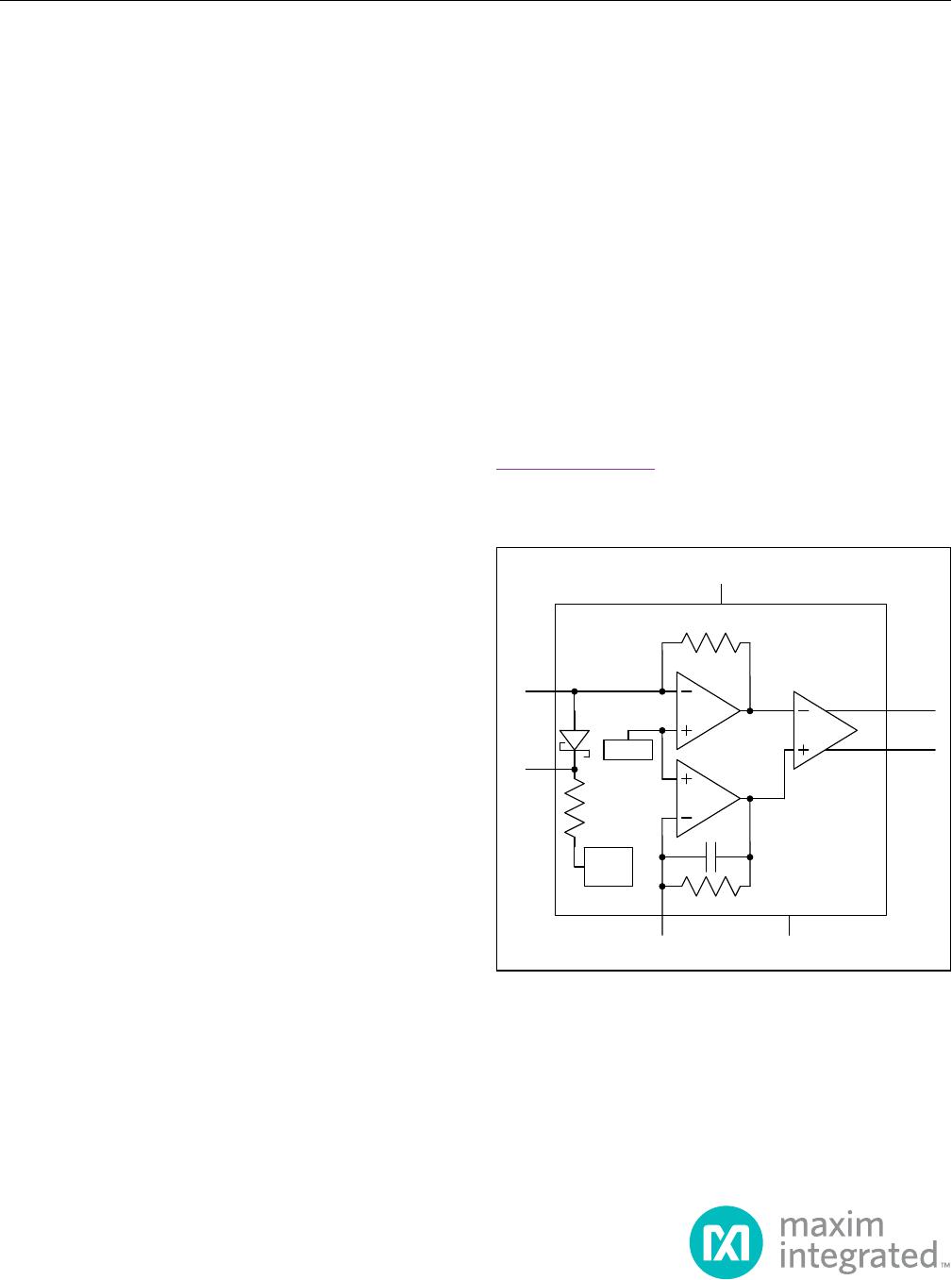
MAX40658/MAX40659 Transimpedance Amplier with 100mA Input
Current Clamp for LiDAR Applications