VS-ST330C04L1

VS-ST330C Series
www.vishay.com
Vishay Semiconductors
Revision: 20-Dec-13
4
Document Number: 94407
For technical questions within your region: DiodesAmericas@vishay.com
, DiodesAsia@vishay.com, DiodesEurope@vishay.com
THIS DOCUMENT IS SUBJECT TO CHANGE WITHOUT NOTICE. THE PRODUCTS DESCRIBED HEREIN AND THIS DOCUMENT
ARE SUBJECT TO SPECIFIC DISCLAIMERS, SET FORTH AT www.vishay.com/doc?91000
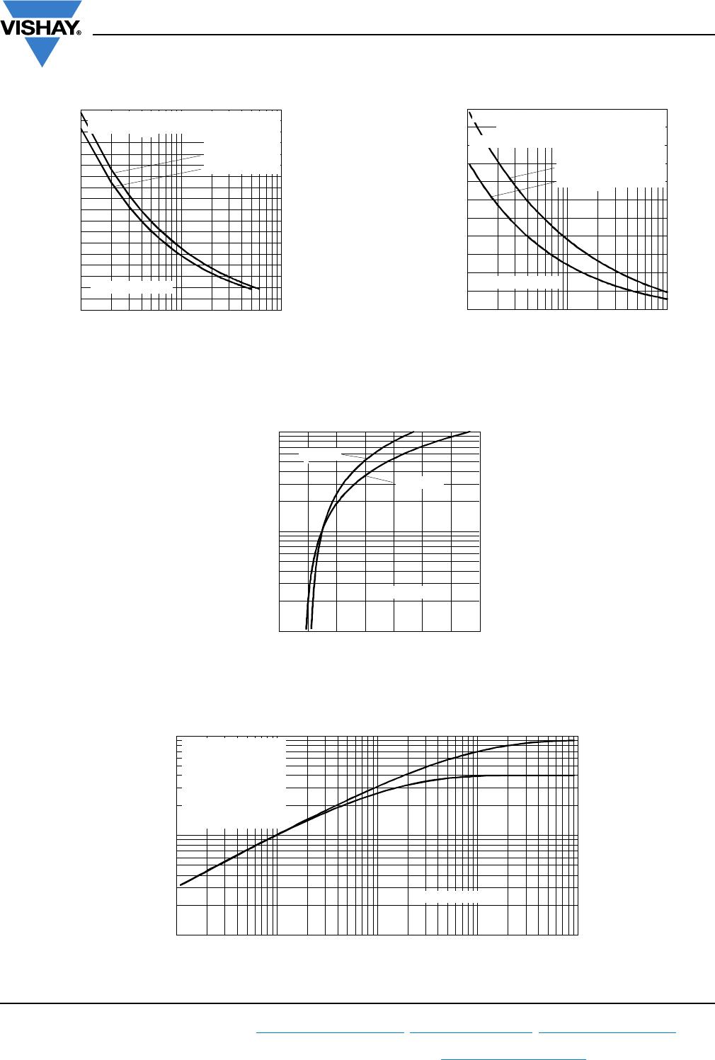
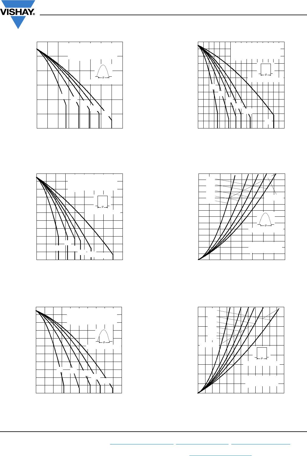
Fig. 1 - Current Ratings Characteristics
Fig. 2 - Current Ratings Characteristics
Fig. 3 - Current Ratings Characteristics
Fig. 4 - Current Ratings Characteristics
Fig. 5 - On-State Power Loss Characteristics
Fig. 6 - On-State Power Loss Characteristics
70
80
90
100
110
120
130
0 50 100 150 200 250 300 350 400
30°
60°
90°
120°
180°
Average On-state Current (A)
Conduction Angle
Maximum Allowable Heatsink Temperature (°C)
ST3 3 0 C . . C Se r i e s
(Single Side Cooled)
R (DC) = 0.09 K/ W
thJ-hs
20
30
40
50
60
70
80
90
100
110
120
130
0 100 200 300 400 500 600 700 800 900
DC
30°
60°
90°
120°
180°
Average On-state Current (A)
Conduction Period
Maximum Allowable Heatsink Temperature (°C)
ST3 3 0 C . . C Se r i e s
(Single Side Cooled)
R (DC) = 0.09 K/W
thJ-hs
20
30
40
50
60
70
80
90
100
110
120
130
0 200 400 600 800 1000
30°
60°
90°
120°
180°
Average On-state Current (A)
Conduction Angle
Maximum Allowable Heatsink TemperatureC)
ST3 3 0 C . . C Se r i e s
(Double Side Cooled)
R (DC) = 0.04 K/ W
thJ-hs
10
20
30
40
50
60
70
80
90
100
110
120
130
0 200 400 600 800 1000 1200 1400 1600
DC
30°
60°
90°
120°
180°
Average On-state Current (A)
Conduction Period
Maximum Allowable Heatsink Temperature (°C
)
ST330C..C Series
(Double Side Cooled)
R (DC) = 0.04 K/ W
thJ-hs
0
200
400
600
800
1000
1200
1400
0 100 200 300 400 500 600 700 800
180°
120°
90°
60°
30°
RM S Li m i t
Conduction Angle
Ma xim um Ave ra g e On -sta t e Pow e r Lo ss (W)
Average On-state Current (A)
ST3 3 0 C . . C Se r i e s
T = 125°C
J
0
200
400
600
800
1000
1200
1400
1600
1800
0 200 400 600 800 1000 1200
DC
180°
120°
90°
60°
30°
RM S Li m i t
Conduction Period
Maximum Average On-state Power Loss (W)
Average On-state Current (A)
ST330C..C Series
T = 125°C
J
VS-ST330C Series
www.vishay.com
Vishay Semiconductors
Revision: 20-Dec-13
5
Document Number: 94407
For technical questions within your region: DiodesAmericas@vishay.com
, DiodesAsia@vishay.com, DiodesEurope@vishay.com
THIS DOCUMENT IS SUBJECT TO CHANGE WITHOUT NOTICE. THE PRODUCTS DESCRIBED HEREIN AND THIS DOCUMENT
ARE SUBJECT TO SPECIFIC DISCLAIMERS, SET FORTH AT www.vishay.com/doc?91000
Fig. 7 - Maximum Non-Repetitive Surge Current
Single and Double Side Cooled
Fig. 8 - Maximum Non-Repetitive Surge Current
Single and Double Side Cooled
Fig. 9 - On-State Voltage Drop Characteristics
Fig. 10 - Thermal Impedance Z
thJ-hs
Characteristics
3500
4000
4500
5000
5500
6000
6500
7000
7500
8000
110100
Number Of Eq ua l Amp litude Half Cycle Current Pulses (N)
Pea k Ha lf S
ine Wave On-state Current (A)
Init ia l T = 125°C
@ 60 Hz 0.0083 s
@ 50 Hz 0.0100 s
J
ST3 3 0 C . . C Se r i e s
At Any Ra ted Loa d Cond ition And With
Rated V Applied Following Surge.
RRM
3500
4000
4500
5000
5500
6000
6500
7000
7500
8000
8500
9000
0.01 0.1 1
Pulse Tra in Du ra t io n (s)
Versus Pulse Train Duration. Control
Peak Half Sine Wave On-state Current (A)
Initial T = 125°C
No Voltage Reapplied
Rated V Reapplied
RRM
J
ST3 3 0 C . . C Se r i e s
Maximum Non Repetitive Surge Current
Of Conduc tion May Not Be Maintained.
100
1000
10000
01234567
T = 2 5° C
J
In st a n t a n eo u s O n -st a t e C urr e n t ( A)
Instantaneous On-state Voltage (V)
T = 1 2 5 ° C
J
ST330C..C Se ries
0.001
0.01
0.1
0.001 0.01 0.1 1 10
Sq u a r e W a v e Pu l se D u r a t i o n ( s )
thJ-hs
St e a d y St a t e V a l u e
R = 0.09 K/ W
(Single Side Cooled)
R = 0.04 K/ W
(Double Side Cooled)
(DC Operation)
thJ-hs
thJ-hs
ST3 3 0 C . . C Se r i e s
Transient Thermal Impedance Z (K/ W)
VS-ST330C Series
www.vishay.com
Vishay Semiconductors
Revision: 20-Dec-13
6
Document Number: 94407
For technical questions within your region: DiodesAmericas@vishay.com
, DiodesAsia@vishay.com, DiodesEurope@vishay.com
THIS DOCUMENT IS SUBJECT TO CHANGE WITHOUT NOTICE. THE PRODUCTS DESCRIBED HEREIN AND THIS DOCUMENT
ARE SUBJECT TO SPECIFIC DISCLAIMERS, SET FORTH AT www.vishay.com/doc?91000
Fig. 11 - Gate Characteristics
ORDERING INFORMATION TABLE
0.1
1
10
100
0.001 0.01 0.1 1 10 100
VGD
IGD
(b)
(a)
Tj = 2 5 ° C
Tj = 12 5 ° C
Tj = - 4 0 ° C
(2)
(3)
Instantaneous Gate Current (A)
In st a n t a n e o us G a t e V o l t a g e ( V )
a) Recommended load line for
b) Recommended load line for
<=30% rated di/dt : 10V, 10ohms
Frequency Limited by PG(AV)
rated di/dt : 20V, 10ohms ; tr<=1 µs
tr<=1 µs
(1)
(1) PGM = 10W, tp = 4 ms
(2) PGM = 20W, tp = 2 ms
(3) PGM = 40W, tp = 1 ms
(4) PGM = 60W, tp = 0.66 ms
Rectangular gate pulse
D e v i c e : ST3 3 0 C . . C Se r i e s
(4)
Device code
51 32 4 6 7 8 9
VS- ST 33 0 C 16 C 1 -
- Thyristor
2
- Essential part number
3
- 0 = Converter grade
4
- C = Ceramic PUK
5
- Voltage code x 100 = V
RRM
(see Voltage Ratings table)
6
- C = PUK case TO-200AB (E-PUK)
7
- 0 = Eyelet terminals (gate and auxiliary cathode unsoldered leads)
1 = Fast-on terminals (gate and auxiliary cathode unsoldered leads)
2 = Eyelet terminals (gate and auxiliary cathode soldered leads)
9
8
- Critical dV/dt:
None = 500 V/µs (standard selection)
L = 1000 V/µs (special selection)
3 = Fast-on terminals (gate and auxiliary cathode soldered leads)
1
- Vishay Semiconductors product
LINKS TO RELATED DOCUMENTS
Dimensions http://www.vishay.com/doc?95075

VS-ST330C04L1

Mfr. #:
Manufacturer:
Vishay Semiconductors
Description:
SCR Modules 650 Amp 400 Volt 1230 Amp IT(RMS)
Lifecycle:
New from this manufacturer.
Delivery:
DHL FedEx Ups TNT EMS
Payment:
T/T Paypal Visa MoneyGram Western Union