Data Sheet AD8000
Rev. C | Page 3 of 17
SPECIFICATIONS WITH ±5 V SUPPLY
At T
A
= 25°C, V
S
= ±5 V, R
L
= 150 Ω, Gain = +2, R
F
= R
G
= 432 Ω, unless otherwise noted. Connect the exposed paddle to ground.
Table 1.
Parameter Test Conditions/Comments Min Typ Max Unit
DYNAMIC PERFORMANCE
−3 dB Bandwidth G = +1, V
O
= 0.2 V p-p, SOIC/LFCSP 1580/1350 MHz
G = +2, V
O
= 2 V p-p, SOIC/LFCSP 650/610 MHz
Bandwidth for 0.1 dB Flatness V
O
= 2 V p-p, SOIC/LFCSP 190/170 MHz
Slew Rate G = +2, V
O
= 4 V step 4100 V/μs
Settling Time to 0.1% G = +2, V
O
= 2 V step 12 ns
NOISE/HARMONIC PERFORMANCE
Second/Third Harmonic V
O
= 2 V p-p, f = 5 MHz, LFCSP only 86/89 dBc
Second/Third Harmonic V
O
= 2 V p-p, f = 20 MHz, LFCSP only 75/79 dBc
Input Voltage Noise f = 100 kHz 1.6 nV/√Hz
Input Current Noise f = 100 kHz, −IN 26 pA/√Hz
f = 100 kHz, +IN 3.4 pA/√Hz
Differential Gain Error NTSC, G = +2 0.02 %
Differential Phase Error NTSC, G = +2 0.01 Degree
DC PERFORMANCE
Input Offset Voltage 1 10 mV
Input Offset Voltage Drift 11 μV/°C
Input Bias Current (Enabled) +I
B
−5 +4 μA
−I
B
−3 +45 μA
Transimpedance 570 890 1600
INPUT CHARACTERISTICS
Noninverting Input Impedance 2/3.6 MΩ/pF
Input Common-Mode Voltage Range −3.5 to +3.5 V
Common-Mode Rejection Ratio V
CM
= ±2.5 V −52 −54 −56 dB
Overdrive Recovery G = +1, f = 1 MHz, triangle wave 30 ns
POWER DOWN PIN
Power-Down Input Voltage Power-down < +V
S
– 3.1 V
Enabled > +V
S
– 1.9 V
Turn-Off Time
50% of power-down voltage to
10% of V
OUT
final, V
IN
= 0.3 V p-p
150 ns
Turn-On Time
50% of power-down voltage to
90% of V
OUT
final, V
IN
= 0.3 V p-p
300 ns
Input Bias Current
Enabled −1.1 +0.17 +1.4 μA
Power-Down −300 −235 −160 μA
OUTPUT CHARACTERISTICS
Output Voltage Swing R
L
= 100 Ω ±3.7 ±3.9 V
Output Voltage Swing R
L
= 1 kΩ ±3.9 ±4.1 V
Linear Output Current V
O
= 2 V p-p, second HD < −50 dBc 100 mA
Overdrive Recovery G = + 2, f = 1 MHz, triangle wave 45 ns
G = +2, V
IN
= 2.5 V to 0 V step 22 ns
POWER SUPPLY
Operating Range 4.5 12 V
Quiescent Current 12.7 13.5 14.3 mA
Quiescent Current (Power-Down) 1.1 1.3 1.65 mA
Power Supply Rejection Ratio −PSRR/+PSRR −56/−61 −59/−63 dB
AD8000 Data Sheet
Rev. C | Page 4 of 17
SPECIFICATIONS WITH +5 V SUPPLY
At T
A
= 25°C, V
S
= 5 V, R
L
= 150 Ω, Gain = +2, R
F
= R
G
= 432 Ω, unless otherwise noted. Connect the exposed paddle to ground.
Table 2.
Parameter Test Conditions/Comments Min Typ Max Unit
DYNAMIC PERFORMANCE
−3 dB Bandwidth G = +1, V
O
= 0.2 V p-p 980 MHz
G = +2, V
O
= 2 V p-p 477 MHz
G = +10, V
O
= 0.2 V p-p 328 MHz
Bandwidth for 0.1 dB Flatness V
O
= 0.2 V p-p 136 MHz
V
O
= 2 V p-p 136 MHz
Slew Rate G = +2, V
O
= 2 V step 2700 V/μs
Settling Time to 0.1% G = +2, V
O
= 2 V step 16 ns
NOISE/HARMONIC PERFORMANCE
Second/Third Harmonic V
O
= 2 V p-p, 5 MHz, LFCSP only 71/71 dBc
Second/Third Harmonic V
O
= 2 V p-p, 20 MHz, LFCSP only 60/62 dBc
Input Voltage Noise f = 100 kHz 1.6 nV/√Hz
Input Current Noise f = 100 kHz, −IN 26 pA/√Hz
f = 100 kHz, +IN 3.4 pA/√Hz
Differential Gain Error NTSC, G = +2 0.01 %
Differential Phase Error NTSC, G = +2 0.06 Degree
DC PERFORMANCE
Input Offset Voltage 1.3 10 mV
Input Offset Voltage Drift 18 μV/°C
Input Bias Current (Enabled) +I
B
−5 +3 μA
−I
B
−1 +45 μA
Transimpedance 440 800 1500
INPUT CHARACTERISTICS
Noninverting Input Impedance 2/3.6 MΩ/pF
Input Common-Mode Voltage Range 1.5 to 3.6 V
Common-Mode Rejection Ratio V
CM
= ±2.5 V −51 −52 −54 dB
Overdrive Recovery G = +1, f = 1 MHz, triangle wave 60 ns
POWER DOWN PIN
Power-Down Input Voltage Power-down < +V
S
− 3.1 V
Enable > +V
S
− 1.9 V
Turn-Off Time
50% of power-down voltage to
10% of V
OUT
final, V
IN
= 0.3 V p-p
200 ns
Turn-On Time
50% of power-down voltage to
90% of V
OUT
final, V
IN
= 0.3 V p-p
300 ns
Input Current
Enabled −1.1 +0.17 +1.4 μA
Power-Down −50 −40 −30 μA
OUTPUT CHARACTERISTICS
Output Voltage Swing R
L
= 100 Ω 1.1 to 3.9 1.05 to 4.1 V
R
L
= 1 kΩ 1 to 4.0 0.85 to 4.15 V
Linear Output Current V
O
= 2 V p-p, second HD < −50 dBc 70 mA
Overdrive Recovery G = +2, f = 100 kHz, triangle wave 65 ns
POWER SUPPLY
Operating Range 4.5 12 V
Quiescent Current 11 12 13 mA
Quiescent Current (Power-Down) 0.7 0.95 1.25 mA
Power Supply Rejection Ratio −PSRR/+PSRR −55/−60 −57/−62 dB
Data Sheet AD8000
Rev. C | Page 5 of 17
ABSOLUTE MAXIMUM RATINGS
Table 3.
Parameter Rating
Supply Voltage 12.6 V
Power Dissipation See Figure 4
Common-Mode Input Voltage Range −V
S
− 0.7 V to +V
S
+ 0.7 V
Differential Input Voltage
V
S
Storage Temperature Range −65°C to +125°C
Operating Temperature Range −40°C to +125°C
Lead Temperature (Soldering, 10 sec) 300°C
Junction Temperature 150°C
Stresses at or above those listed under Absolute Maximum Ratings
may cause permanent damage to the product. This is a stress
rating only; functional operation of the product at these or any
other conditions above those indicated in the operational section of
this specification is not implied. Operation beyond the maximum
operating conditions for extended periods may affect product
reliability.
THERMAL RESISTANCE
θ
JA
is specified for the worst-case conditions, that is, θ
JA
is speci-
fied for device soldered in the circuit board for surface-mount
packages.
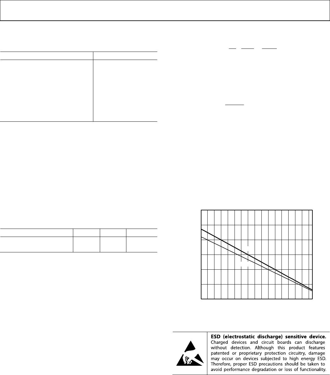
Table 4. Thermal Resistance
Package Type θ
JA
θ
JC
Unit
8-Lead SOIC 80 30 °C/W
3 mm × 3 mm LFCSP 93 35 °C/W
MAXIMUM POWER DISSIPATION
The maximum safe power dissipation for the AD8000 is limited
by the associated rise in junction temperature (T
J
) on the die. At
approximately 150C, which is the glass transition temperature,
the properties of the plastic change. Even temporarily exceeding
this temperature limit can change the stresses that the package
exerts on the die, permanently shifting the parametric performance
of the AD8000. Exceeding a junction temperature of 175C for
an extended period of time can result in changes in silicon de-
vices, potentially causing degradation or loss of functionality.
The power dissipated in the package (P
D
) is the sum of the qui-
escent power dissipation and the power dissipated in the die
due to the AD8000 drive at the output. The quiescent power is
the voltage between the supply pins (V
S
) times the quiescent
current (I
S
).
P
D
= Quiescent Power + (Total Drive PowerLoad Power)

L
2
OUT
L
OUTS
SS
D
R
V
R
V
2
V
IVP
Consider the RMS output voltages. If R
L
is referenced to −V
S
, as
in single-supply operation, the total drive power is V
S
× I
OUT
. If
the rms signal levels are indeterminate, consider the worst case,
when V
OUT
= V
S
/4 for R
L
to midsupply.

L
S
SS
D
R
/V
IVP
2
4
In single-supply operation with R
L
referenced to −V
S
, worst case
is V
OUT
= V
S
/2.
Airflow increases heat dissipation, effectively reducing θ
JA
. Also,
more metal directly in contact with the package leads and exposed
paddle from metal traces, through holes, ground, and power
planes reduces θ
JA
.
Figure 4 shows the maximum safe power dissipation in the
package vs. the ambient temperature for the exposed paddle
SOIC (80°C/W) and the LFCSP (93°C/W) package on a JEDEC
standard 4-layer board. θ
JA
values are approximations.
0
0.5
1.0
1.5
2.0
2.5
3.0
MAXIMUM POWER DISSIPATION (W)
05321-063
–30 –20 –10 0 10 20 40 8030 50 60 70 10090 120110
AMBIENT TEMPERATURE (C)
SOIC
LFCSP
–40
Figure 4. Maximum Power Dissipation vs. Temperature for a 4-Layer Board
ESD CAUTION

AD8000YRDZ-REEL

Mfr. #:
Manufacturer:
Analog Devices Inc.
Description:
IC OPAMP CFA 1.58GHZ 8SOIC
Lifecycle:
New from this manufacturer.
Delivery:
DHL FedEx Ups TNT EMS
Payment:
T/T Paypal Visa MoneyGram Western Union