MAX5401EKA+T

General Description
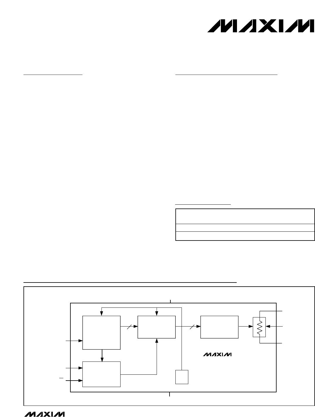
The MAX5400/MAX5401 digital potentiometers offer
256-tap SOT-PoT™ digitally controlled variable resis-
tors in tiny 8-pin SOT23 packages. Each device func-
tions as a mechanical potentiometer, consisting of a
fixed resistor string with a digitally controlled wiper con-
tact. They operate from +2.7V to +5.5V single-supply
voltages and use an ultra-low supply current of 0.1µA.
These devices also provide glitchless switching
between resistor taps, as well as a convenient power-
on reset that sets the wiper to the midscale position at
power-up. A low 5ppm/°C ratiometric temperature coef-
ficient makes it ideal for applications requiring low drift.
The MAX5400/MAX5401 serve well in applications
requiring digitally controlled resistors, including
adjustable voltage references and programmable gain
amplifiers (PGAs). A nominal end-to-end resistor tem-
perature coefficient of 50ppm/°C allows these parts to
be used as variable resistors in applications such as
low-tempco adjustable gain and other circuit configura-
tions.
Two resistance values are available: 50k (MAX5400)
and 100k (MAX5401). Each device is guaranteed over
the extended industrial temperature range (-40°C to
+85°C).
________________________Applications
Mechanical Potentiometer Replacement
Low-Drift PGAs
Adjustable Voltage References
Features
Miniature 8-Pin SOT23 (3mm x 3mm)
256 Tap Positions
Ultra-Low 0.1µA Supply Current
Single-Supply Operation: +2.7V to +5.5V
Low Ratiometric Temperature Coefficient:
5ppm/°C
Power-On Reset: Wiper Goes to Midscale
(Position 128)
Glitchless Switching Between the Resistor Taps
3-Wire SPI™-Interface Compatible
50k/100k Resistor Values
MAX5400/MAX5401
256-Tap SOT-PoT,
Low-Drift Digital Potentiometers in SOT23
________________________________________________________________ Maxim Integrated Products 1
19-1848; Rev 0; 10/00
Ordering Information
SOT-PoT is a trademark of Maxim Integrated Products.
SPI is a trademark of Motorola, Inc.
Pin Configuration appears at end of data sheet.
PART
TEMP.
RANGE
PIN-
PACKAGE
R (k)
MAX5400EKA-T -40°C to +85°C 8-SOT23 50
MAX5401EKA-T -40°C to +85°C 8-SOT23 100
For price, delivery, and to place orders, please contact Maxim Distribution at 1-888-629-4642,
or visit Maxim’s website at www.maxim-ic.com.
MAX5400/MAX5401
POR
8
8-BIT
SHIFT
REGISTER
CLOCK
LOGIC
8-BIT
LATCH
SCLK
DIN
CS
8
H
W
L
DECODER
V
DD
GND
Functional Diagram
MAX5400/MAX5401
256-Tap SOT-PoT,
Low-Drift Digital Potentiometers in SOT23
2 _______________________________________________________________________________________
ABSOLUTE MAXIMUM RATINGS
ELECTRICAL CHARACTERISTICS
(V
DD
= +5V, V
H
= V
DD
, V
L
= 0, T
A
= T
MIN
to T
MAX
. Typical values are at T
A
= +25°C, unless otherwise noted. Parameters are mea-
sured at T
A
= +25°C. Values over full temperature range are guaranteed by design.)
Stresses beyond those listed under “Absolute Maximum Ratings” may cause permanent damage to the device. These are stress ratings only, and functional
operation of the device at these or any other conditions beyond those indicated in the operational sections of the specifications is not implied. Exposure to
absolute maximum rating conditions for extended periods may affect device reliability.
V
DD
to GND............................................................. -0.3V to +6V
DIN, SCLK, CS to GND ............................................-0.3V to +6V
H, L, W to GND...........................................-0.3V to (V
DD
+ 0.3V)
Maximum Continuous Current into
Pins H, L, and W ...........................................................±1mA
Continuous Power Dissipation (T
A
= +70°C)
8-Pin SOT23 (derate 8.7mW/°C above +70°C)...........697mW
Operating Temperature Range ...........................-40°C to +85°C
Junction Temperature ..................................................+150°C
Storage Temperature Range .............................-65°C to +150°C
Lead Temperature (soldering, 10s) .................................+300°C
PARAMETER SYMBOL CONDITIONS MIN TYP MAX UNITS
DC PERFORMANCE (Voltage Divider Mode)
Resolution N 8 Bits
Integral Nonlinearity
(Notes 1, 2)
INL ±1/2 LSB
Differential Nonlinearity
(Notes 1, 2)
DNL ±1/2 LSB
End-to-End Resistor Tempco TC
R
50 ppm/°C
Ratiometric Resistor Tempco 5 ppm/°C
MAX5400 -0.8
Full-Scale Ratio Error
MAX5401 -0.4
LSB
MAX5400 +0.8
Zero-Scale Ratio Error
MAX5401 +0.4
LSB
POWER SUPPLIES
Supply Voltage V
DD
2.7 5.5 V
V
DD
= 5V 0.7 5 µA
Supply Current I
DD
CS = SCLK = DIN = V
DD
V
DD
= 2.7V 0.1 µA
DC PERFORMANCE (Variable Resistor Mode)
Resolution N 8 Bits
V
CC
= 5V ±1
MAX5400 ±1.5
Integral Nonlinearity
(Notes 1, 3)
INL
V
CC
= 3V
MAX5401 ±1
LSB
V
CC
= 5V ±1/2
Differential Nonlinearity
(Notes 1, 3)
DNL
V
CC
= 3V ±1/2
LSB
DC PERFORMANCE (Resistor Characteristics)
Wiper Resistance (Note 4) R
W
250 800
Wiper Capacitance C
W
25 pF
MAX5401 75 100 125
End-to-End Resistance R
HL
MAX5400 37.5 50 62.5
k
MAX5400/MAX5401
256-Tap SOT-PoT,
Low-Drift Digital Potentiometers in SOT23
_______________________________________________________________________________________ 3
Note 1: Linearity is defined in terms of the H to L code-dependent resistance.
Note 2: The DNL and INL are measured with the potentiometer configured as a voltage-divider with H = V
DD
and L = 0. The wiper
terminal is unloaded and measured with an ideal voltmeter.
Note 3: The DNL and INL are measured with the potentiometer configured as a variable resistor. H is unconnected and L = 0. The
wiper terminal is driven with a source current of 80µA for the 50k configuration and 40µA for the 100k configuration.
Note 4: The wiper resistance is measured assuming the source currents given in Note 2.
Note 5: Digital timing is guaranteed by design.
PARAMETER SYMBOL CONDITIONS MIN TYP MAX UNITS
DIGITAL INPUTS
Input High Voltage V
IH
V
CC
= 5V 0.7
V
DD
V
Input Low Voltage V
IL
V
CC
= 5V 0.3
V
DD
V
Input High Voltage V
IH
V
CC
= 3V 0.7
V
DD
V
Input Low Voltage V
IL
V
CC
= 3V 0.3
V
DD
V
Input Leakage Current ±1.0 µA
Input Capacitance 5.0 pF
TIMING CHARACTERISTICS (Voltage Divider Mode)
MAX5400 (to 50% of final value, from code 0
to code 128)
300
Wiper Settling Time t
IL
MAX5401 (to 50% of final value, from code 0
to code 128)
600
ns
TIMING CHARACTERISTICS (Digital) (Note 5)
SCLK Clock Period t
CP
100 ns
SCLK Pulse Width High t
CH
40 ns
SCLK Pulse Width Low t
CL
40 ns
CS Fall to SCLK Rise Setup
Time
t
CSS
40 ns
SCLK Rise to CS Rise Hold Time t
CSH
0ns
DIN Setup Time t
DS
40 ns
DIN Hold Time t
DH
0ns
SCLK Rise to CS Fall Delay t
CS0
10 ns
CS Rise to SCLK Rise Hold t
CS1
40 ns
CS Pulse Width High t
CSW
100 ns
ELECTRICAL CHARACTERISTICS (continued)
(V
DD
= +5V, V
H
= V
DD
, V
L
= 0, T
A
= T
MIN
to T
MAX
. Typical values are at T
A
= +25°C, unless otherwise noted. Parameters are mea-
sured at T
A
= +25°C. Values over full temperature range are guaranteed by design.)

MAX5401EKA+T

Mfr. #:
Manufacturer:
Maxim Integrated
Description:
Digital Potentiometer ICs 256-Tap Low-Drift
Lifecycle:
New from this manufacturer.
Delivery:
DHL FedEx Ups TNT EMS
Payment:
T/T Paypal Visa MoneyGram Western Union

Products related to this Datasheet