LTC3105
8
3105fb
For more information www.linear.com/LTC3105
Introduction
The LTC3105 is a unique, high performance, synchronous
boost converter that incorporates maximum power point
control, 250mV start-up capability and an integrated LDO
regulator. This part operates over a very wide range of input
voltages from 225mV to 5V. Its Burst Mode architecture
and low 24µA quiescent current optimize efficiency in low
power applications.
An integrated maximum power point controller allows for
operation directly from high impedance sources such as
photovoltaic cells by preventing the input power source
voltage from collapsing below the user programmable
MPPC threshold. Peak current limits are automatically
adjusted with proprietary techniques to maintain operation
at levels that maximize power extraction from the source.
The 250mV start-up voltage and 225mV minimum
operating voltage enable direct operation from a single
photovoltaic cell and other very low voltage, high series
impedance power sources such as TEGs and fuel cells.
Synchronous rectification provides high efficiency opera
-
tion while eliminating the need for external Schottky diodes.
The L
TC3105 provides output disconnect which prevents
large inrush currents during start-up. This is particularly
important
for high internal resistance power sources like
photovoltaic cells and thermoelectric generators which
can become overloaded if inrush current is not limited
during start-up of the power converter. In addition, output
disconnect isolates V
OUT
from V
IN
while in shutdown.
V
IN
> V
OUT
Operation
The LTC3105 includes the ability to seamlessly maintain
regulation if V
IN
becomes equal to or greater than V
OUT
.
With V
IN
greater than or equal to V
OUT
, the synchro-
nous rectifiers are disabled which may result in reduced
efficiency.
Shutdown Control
The SHDN pin is an active low input that places the IC
into low current shutdown mode. This pin incorporates an
internal 2MΩ pull-up resistor which enables the converter
if the SHDN pin is not controlled by an external circuit. The
SHDN pin should be allowed to float while the part is in
OPERATION
start-up mode. Once in normal operation, the SHDN pin
may be controlled using an open-drain or open-collector
pull-down. Other external loads on this pin should be
avoided, as they may result in the part failing to reach
regulation. In shutdown, the internal switch connecting
AUX and V
OUT
is enabled.
When the SHDN pin is released, the LTC3105 is enabled
and begins switching after a short delay. When either V
IN
or V
AUX
is above 1.4V, this delay will typically range be-
tween 20µs and 100µs. Refer to the Typical Performance
Characteristics section for more details.
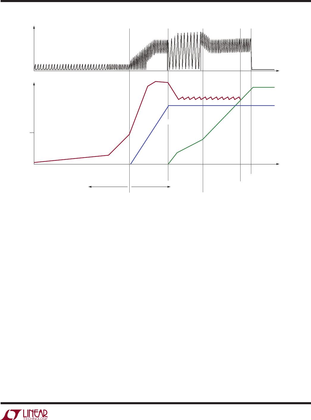
Start-Up Mode Operation
The LTC3105 provides the capability to start with voltages
as low as 250mV
. During start-up the AUX output initially
is charged with the synchronous rectifiers disabled. Once
V
AUX
has reached approximately 1.4V, the converter leaves
start-up mode and enters normal operation. Maximum
power point control is not enabled during start-up, however,
the currents are internally limited to sufficiently low levels
to allow start-up from weak input sources.
While the converter is in start-up mode, the internal switch
between AUX and V
OUT
remains disabled and the LDO
is disabled. Refer to Figure 1 for an example of a typical
start-up sequence.
The LTC3105 is optimized for use with high impedance
power sources such as photovoltaic cells. For operation
from very low impedance, low input voltage sources, it may
be necessary to add several hundred milliohms of series
input resistance to allow for proper low voltage start-up.
Normal Operation
When either V
IN
or V
AUX
is greater than 1.4V typical, the
converter will enter normal operation.
The converter continues charging the AUX output until
the LDO output enters regulation. Once the LDO output
is in regulation, the converter begins charging the V
OUT
pin. V
AUX
is maintained at a level sufficient to ensure the
LDO remains in regulation. If V
AUX
becomes higher than
required to maintain LDO regulation, charge is transferred
from the AUX output to the V
OUT
output. If V
AUX
falls too
low, current is redirected to the AUX output instead of
being used to charge the V
OUT
output. Once V
OUT
rises