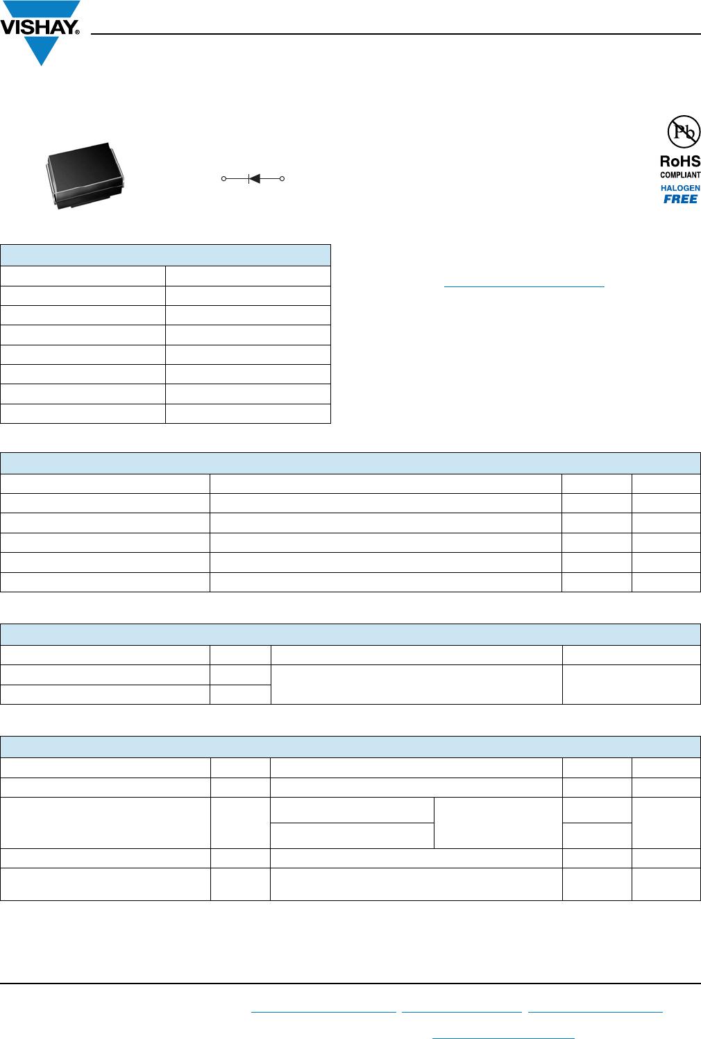
VS-10BQ060-M3/5BT

VS-10BQ060-M3
www.vishay.com
Vishay Semiconductors
Revision: 27-Oct-15
1
Document Number: 93357
For technical questions within your region: DiodesAmericas@vishay.com
, DiodesAsia@vishay.com, DiodesEurope@vishay.com
THIS DOCUMENT IS SUBJECT TO CHANGE WITHOUT NOTICE. THE PRODUCTS DESCRIBED HEREIN AND THIS DOCUMENT
ARE SUBJECT TO SPECIFIC DISCLAIMERS, SET FORTH AT www.vishay.com/doc?91000
High Performance Schottky Rectifier, 1.0 A
FEATURES
Low forward voltage drop
Guard ring for enhanced ruggedness and
long term reliability
Small foot print, surface mountable
High frequency operation
Meets MSL level 1, per J-STD-020, LF maximum peak
of 260 °C
Material categorization: for definitions of compliance
please see www.vishay.com/doc?99912
DESCRIPTION
The VS-10BQ060-M3 surface mount Schottky rectifier has
been designed for applications requiring low forward drop
and very small foot prints on PC boards. Typical
applications are in disk drives, switching power supplies,
converters, freewheeling diodes, battery charging, and
reverse battery protection.
PRODUCT SUMMARY
I
F(AV)
1.0 A
V
R
60 V
V
F
at I
F
0.42 V
I
RM
8 mA at 125 °C
T
J
max. 150 °C
E
AS
2.0 mJ
Package SMB
Diode variation Single die
Cathode Anode
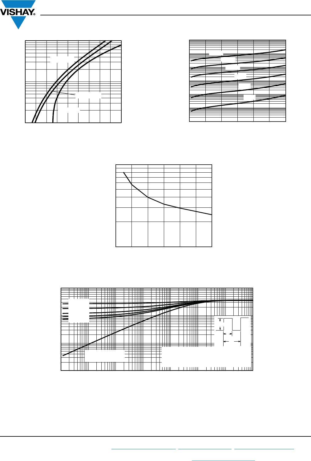
MAJOR RATINGS AND CHARACTERISTICS
SYMBOL CHARACTERISTICS VALUES UNITS
I
F(AV)
Rectangular waveform 1.0 A
V
RRM
60 V
I
FSM
t
p
= 5 μs sine 700 A
V
F
1.0 A
pk
, T
J
= 125 °C 0.42 V
T
J
Range -55 to +150 °C
VOLTAGE RATINGS
PARAMETER SYMBOL VS-10BQ060-M3 UNITS
Maximum DC reverse voltage V
R
60 V
Maximum working peak reverse voltage V
RWM
ABSOLUTE MAXIMUM RATINGS
PARAMETER SYMBOL TEST CONDITIONS VALUES UNITS
Maximum average forward current I
F(AV)
50 % duty cycle at T
L
= 116 °C, rectangular waveform 1.0 A
Maximum peak one cycle
non-repetitive surge current
I
FSM
5 μs sine or 3 μs rect. pulse
Following any rated
load condition and with
rated V
RRM
applied
700
A
10 ms sine or 6 ms rect. pulse 42
Non-repetitive avalanche energy E
AS
T
J
= 25 °C, I
AS
= 1 A, L = 4 mH 2.0 mJ
Repetitive avalanche current I
AR
Current decaying linearly to zero in 1 μs
Frequency limited by T
J
maximum V
A
= 1.5 x V
R
typical
1.0 A
VS-10BQ060-M3
www.vishay.com
Vishay Semiconductors
Revision: 27-Oct-15
2
Document Number: 93357
For technical questions within your region: DiodesAmericas@vishay.com
, DiodesAsia@vishay.com, DiodesEurope@vishay.com
THIS DOCUMENT IS SUBJECT TO CHANGE WITHOUT NOTICE. THE PRODUCTS DESCRIBED HEREIN AND THIS DOCUMENT
ARE SUBJECT TO SPECIFIC DISCLAIMERS, SET FORTH AT www.vishay.com/doc?91000
Note
(1)
Pulse width = 300 μs, duty cycle = 2 %
Notes
(1)
thermal runaway condition for a diode on its own heatsink
(2)
Mounted 1" square PCB
ELECTRICAL SPECIFICATIONS
PARAMETER SYMBOL TEST CONDITIONS VALUES UNITS
Maximum forward voltage drop
See fig. 1
V
FM
(1)
1 A
T
J
= 25 °C
0.49
V
2 A 0.60
1 A
T
J
= 125 °C
0.42
2 A 0.56
Maximum reverse leakage current
See fig. 2
I
RM
T
J
= 25 °C
V
R
= Rated V
R
0.1
mA
T
J
= 125 °C 8.0
Typical junction capacitance C
T
V
R
= 5 V
DC
(test signal range 100 kHz to 1 MHz), 25 °C 80 pF
Typical series inductance L
S
Measured lead to lead 5 mm from package body 2.0 nH
Maximum voltage rate of charge dV/dt Rated V
R
10 000 V/μs
THERMAL - MECHANICAL SPECIFICATIONS
PARAMETER SYMBOL TEST CONDITIONS VALUES UNITS
Maximum junction and storage
temperature range
T
J
(1)
, T
Stg
-55 to +150 °C
Maximum thermal resistance,
junction to lead
R
thJL
(2)
DC operation 36
°C/W
Maximum thermal resistance,
junction to ambient
R
thJA
80
Approximate weight
0.10 g
0.003 oz.
Marking device Case style SMB (similar DO-214AA) 1H
dP
tot
dT
J
-------------
1
R
thJA
--------------<
VS-10BQ060-M3
www.vishay.com
Vishay Semiconductors
Revision: 27-Oct-15
3
Document Number: 93357
For technical questions within your region: DiodesAmericas@vishay.com
, DiodesAsia@vishay.com, DiodesEurope@vishay.com
THIS DOCUMENT IS SUBJECT TO CHANGE WITHOUT NOTICE. THE PRODUCTS DESCRIBED HEREIN AND THIS DOCUMENT
ARE SUBJECT TO SPECIFIC DISCLAIMERS, SET FORTH AT www.vishay.com/doc?91000
Fig. 1 - Maximum Forward Voltage Drop Characteristics Fig. 2 - Typical Peak Reverse Current vs.
Reverse Voltage
Fig. 3 - Typical Junction Capacitance vs. Reverse Voltage
Fig. 4 - Maximum Thermal Impedance Z
thJC
Characteristics (Per Leg)
V
FM
-
Forward Voltage Drop (V)
I
F
- Instantaneous Forward Current (A)
0.1 0.2 0.3 0.4 0.5 0.6 0.7 0.8 0.9 1.0
0.1
1
10
T
J
= 25 °C
T
J
= 125 °C
T
J
= 150 °C
V
R
-
Reverse Voltage (V)
I
R
- Reverse Current (mA)
0 10 20 30 40 50 60
0.00010
0.0010
0.010
0.10
1.0
10
100
25 °C
125 °C
150 °C
100 °C
75 °C
50 °C
100
V
R
- Reverse Voltage (V)
C
T
- Junction Capacitance (pF)
0
10
6010
20 40
5030
Z
thJC
-
Thermal Impedance (°C/W)
t
1
-
Rectangular Pulse Duration (s)
0.1
1
10
1
00
0.00001 0.0001 0.001 0.01 0.1 1 10 100
Single pulse
(thermal resistance)
D = 0.75
D = 0.50
D = 0.33
D = 0.25
D = 0.20
2
t
1
t
P
DM
Notes:
1. Duty factor D = t
1
/ t
2
.
2. Peak T
J
= P
dm
x Z
thJC
+ T
c
.

VS-10BQ060-M3/5BT

Mfr. #:
Manufacturer:
Vishay Semiconductors
Description:
Schottky Diodes & Rectifiers 1A 60V Single Die Schottky Rectifier
Lifecycle:
New from this manufacturer.
Delivery:
DHL FedEx Ups TNT EMS
Payment:
T/T Paypal Visa MoneyGram Western Union

Products related to this Datasheet