LT3791
19
3791fb
For more information www.linear.com/LT3791
For loop stability a lowpass RC filter is needed. For
most applications, a 50Ω resistor and 470nF capacitor
is sufficient.
Table 3
R
IN
(mΩ) I
LIMIT
(A)
20 2.5
15 3.3
12 4.2
10 5.0
6 8.3
5 10.0
4 12.5
3 16.7
2 25
IVINMON
The IVINMON pin provides a linear indication of the current
flowing through the input. The equation for V
IVINMON
is
V
(IVINP-IVINN)
20. This pin is suitable for driving an ADC
input, however, the output impedance of this pin is 12.5
so care must be taken not to load this pin.
Programming Output Overvoltage Threshold for Open
LED Protection
For an LED driver application with small output capacitors,
the output voltage usually overshoots a lot during an open
LED event. Although the 1.2V (typical) FB regulation loop
tries to regulate the output, the loop is usually too slow to
prevent the output from overshooting. Once the FB voltage
hits its overvoltage threshold, 1.25V (typical), the LT3791
stops switching by turning TG1, TG2 off, and BG1, BG2
on. In this way, the minimum overshoot is guaranteed.
The output overvoltage threshold can be set by selecting
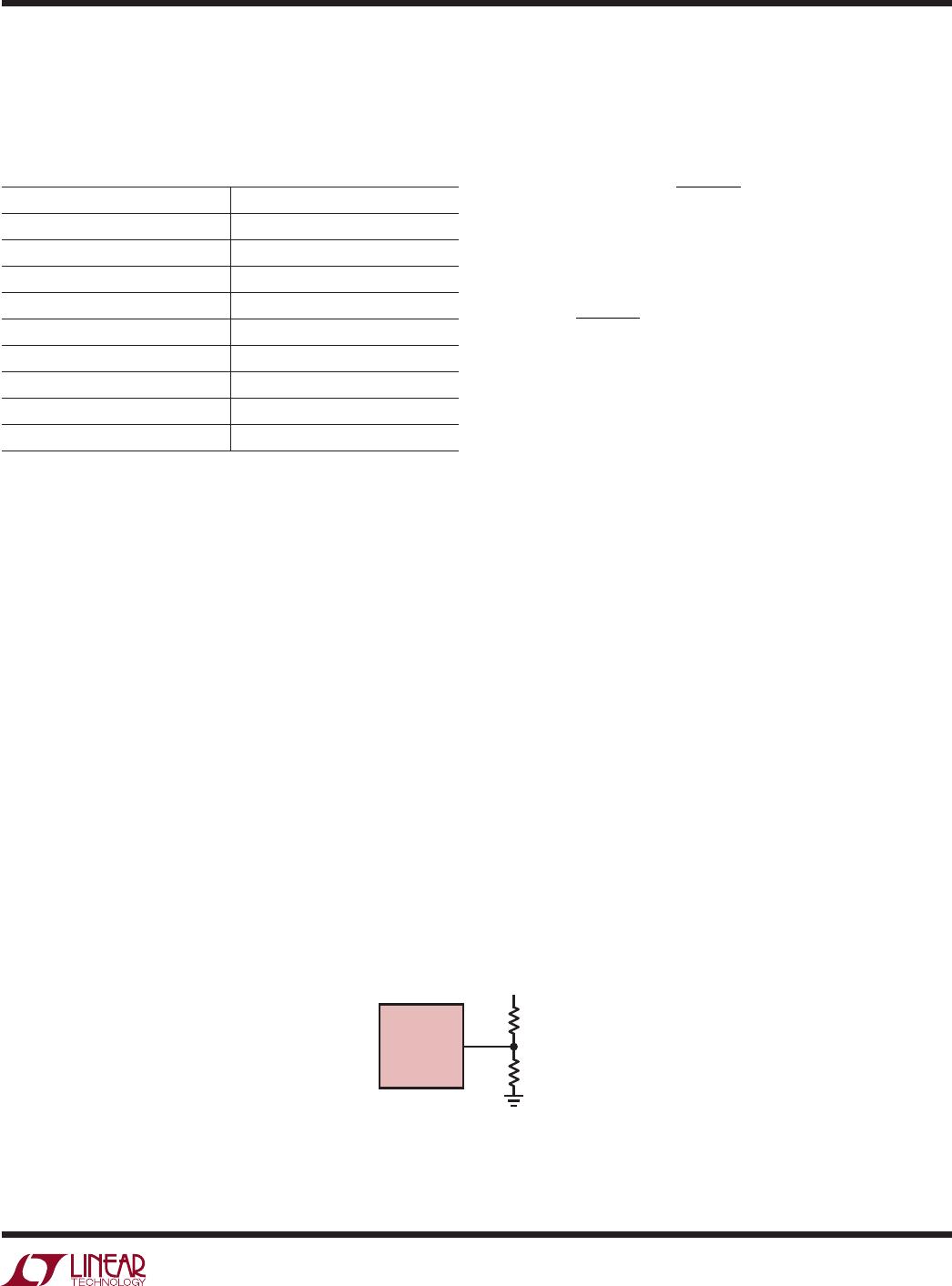
the values of R5 and R6 (see Figure 9) according to the
following equation:
V
OUT(OVP)
= 1.25
R5+ R6
R6
Make sure the expected V
FB
during normal operation does
not exceed 1.1V:
V
LED
R6
R5+R6
1.
1
These equations set the maximum LED string voltage with
open LED protection for the LT3791 to be 52V.
Dimming Control
There are two methods to control the current source for
dimming using the LT3791. One method uses the CTRL
pin to adjust the current regulated in the LEDs. A second
method uses the PWM pin to modulate the current source
between zero and full current to achieve a precisely pro-
grammed average
current. To make PWM dimming more
accurate, the switch demand current is stored on the V
C
node during the quiescent phase when PWM is low. This
feature minimizes recovery time when the PWM signal goes
high. To further improve the recovery time a disconnect
switch may be used in the LED current path to prevent the
ISP node from discharging during the PWM signal low
phase. The minimum PWM on- or off-time is affected by
choice of operating frequency and external component
selection. The best overall combination of PWM and
analog dimming capabilities is available if the minimum
PWM pulse is at least six switching cycles and the PWM
pulse is synchronized to the SYNC signal.
applicaTions inForMaTion
Figure 9. Resistor Connection for Open LED Protection
LT3791
V
OUT
R5
R6
3791 F09
FB
LT3791
20
3791fb
For more information www.linear.com/LT3791
SHORTLED Pin
The LT3791 provides an open-drain status pin,
SHORTLED, which
pulls low when the FB pin is below
400mV. The only time the FB pin will be below 400mV
is during start-up or if the LEDs are shorted. During
start-up the LT3791 ignores the voltage on the FB pin
until the soft-start capacitor reaches 1.75V. To prevent
false tripping after startup, a large enough soft-start
capacitor must be used to allow the output to get up to
approximately 40% to 50% of the final value.
OPENLED Pin
The LT3791 provides an open-drain status pin, OPENLED,
which pulls low when the FB pin is above 1.15V and the
voltage across V
(ISP-ISN)
is less than 10mV. If the open
LED clamp voltage is programmed correctly using the FB
pin, then the FB pin should never exceed 1.1V when the
LEDs are connected. Therefore, the only way for the FB
pin to exceed 1.15V is for an open LED event to occur.
Soft-Start, Fault Function
Soft-start reduces the input power sources’ surge currents
by gradually increasing the controller’s current limit (pro
-
portional to
an internally buffered clamped equivalent of
V
C
). The soft-start interval is set by the soft-start capacitor
selection according to the following equation
t
SS
=
1.2V
14µA
C
SS
Make sure C
SS
is large enough when there is loading
during start-up.
The SS pin is also used as a fault timer. Once an open
LED or a shorted LED fault is detected, a 1.4µA pull-
down current
source is activated. With a 500k pull-up
resistor to V
REF
on the SS pin, the LT3791 will latch off
until the EN/UVLO pin is toggled. Without any resistor
to V
REF
the SS pin enters a hiccup mode operation. The
1.4µA pulls SS down until 0.2V is reached, at which
point
the 14µ
A pull-up current source turns on. If the
fault condition
hasn’t been removed when SS reaches
1.75V, then the 1.4µA pull-down current source turns on
again initiating a new cycle. This will continue until the
fault is removed.
Loop Compensation
The LT3791 uses an internal transconductance error
amplifier whose V
C
output compensates the control loop.
The external inductor, output capacitor and the comp-
ensation resistor
and
capacitor determine the loop
stability.
The
inductor and output capacitor are chosen based on
performance, size and cost. The compensation resis
-
tor and capacitor at V
C
are set to optimize control loop
response and
stability. For typical LED applications, a
10nF compensation
capacitor at V
C
is adequate, and a
series resistor should always be used to increase the
slew rate on the V
C
pin to maintain tighter regulation of
LED current during fast transients on the input supply of
the converter.
applicaTions inForMaTion
LT3791
21
3791fb
For more information www.linear.com/LT3791
Power MOSFET Selections and Efficiency
Considerations
The LT3791 requires four external N-channel power MOS
-
FETs, two for the top switches (switch M1 and M4, shown in
Figure 1) and two for the bottom switches (switch M2 and
M3 shown in Figure 1). Important parameters for the power
MOSFETs are the breakdown voltage, V
BR(DSS)
, threshold
voltage, V
GS(TH)
, on-resistance, R
DS(ON)
, reverse transfer
capacitance, C
RSS
, and maximum current, I
DS(MAX)
.
The drive voltage is set by the 5V INTV
CC
supply. Con-
sequently, logic-level
threshold MOSFETs must be used
in LT3791 applications. If the input voltage is expected
to drop below the 5V, then sub-logic threshold MOSFETs
should be considered.
In order to select the power MOSFETs, the power dis
-
sipated by
the device must be known. For switch M1, the
maximum
power dissipation happens in boost operation,
when it remains on all the time. Its maximum power dis
-
sipation at maximum output current is given by:
P
M1(BOOST)
=
I
LED
V
OUT
V
IN
2
ρ
T
R
DS(ON)
where ρ
T
is a normalization factor (unity at 25°C)
accounting for
the significant variation in on-resistance
with temperature, typically 0.4%/°C as shown in Figure
10. For a maximum junction temperature of 125°C, using
a value of ρ
T
= 1.5 is reasonable.
Switch M2 operates in buck operation as the synchronous
rectifier. Its power dissipation at maximum output current
is given by:
P
M2(BUCK)
=
V
IN
V
OUT
V
IN
I
LED
2
ρ
T
R
DS(ON)
Switch M3 operates in boost operation as the control
switch. Its power dissipation at maximum current is
given by:
P
M3(BOOST)
=
V
OUT
V
IN
( )
V
OUT
V
IN
2
I
LED
2
ρ
T
R
DS(ON)
+ k V
OUT
3
I
LED
V
IN
C
ROSS
f
where C
RSS
is usually specified by the MOSFET manufac-
turers. The constant k, which accounts for the loss caused
by
reverse-recovery current, is inversely proportional to
the gate drive current and has an empirical value of 1.7.
For switch M4, the maximum power dissipation happens
in boost operation, when its duty cycle is higher than
50%. Its maximum power dissipation at maximum output
current is given by:
P
M4(BOOST)
=
V
IN
V
OUT
I
LED
V
OUT
V
IN
2
ρ
T
R
DS(ON)
For the same output voltage and current, switch M1 has
the highest power dissipation and switch M2 has the low-
est power
dissipation unless a short occurs at the output.
applicaTions inForMaTion

LT3791IFE#PBF

Mfr. #:
Manufacturer:
Analog Devices / Linear Technology
Description:
LED Lighting Drivers 60V 4-Switch Sync Buck-Boost LED Drvr Cn
Lifecycle:
New from this manufacturer.
Delivery:
DHL FedEx Ups TNT EMS
Payment:
T/T Paypal Visa MoneyGram Western Union