AVAILABLE
Functional Diagrams
Pin Configurations appear at end of data sheet.
Functional Diagrams continued at end of data sheet.
UCSP is a trademark of Maxim Integrated Products, Inc.
For pricing, delivery, and
ordering information, please contact Maxim Direct
at 1-888-629-4642, or visit Maxim’s website at www.maximintegrated.com.
3.3V/5V/Adjustable-Output,
Step-Up DC-DC Converters
_______________General Description
The MAX756/MAX757 are CMOS step-up DC-DC switch-
ing regulators for small, low input voltage or battery-pow-
ered systems. The MAX756 accepts a positive input
voltage down to 0.7V and converts it to a higher pin-
selectable output voltage of 3.3V or 5V. The MAX757 is
an adjustable version that accepts an input voltage down
to 0.7V and generates a higher adjustable output voltage
in the range from 2.7V to 5.5V. Typical full-load efficiencies
for the MAX756/MAX757 are greater than 87%.
The MAX756/MAX757 provide three improvements over
previous devices. Physical size is reduced—the high
switching frequencies (up to 0.5MHz) made possible by
MOSFET power transistors allow for tiny (<5mm diameter)
surface-mount magnetics. Efficiency is improved to 87%
(10% better than with low-voltage regulators fabricated in
bipolar technology). Supply current is reduced to 60µA
by CMOS construction and a unique constant-off-time
pulse-frequency modulation control scheme.
________________________Applications
3.3V to 5V Step-Up Conversion
Palmtop Computers
Portable Data-Collection Equipment
Personal Data Communicators/Computers
Medical Instrumentation
2-Cell & 3-Cell Battery-Operated Equipment
Glucose Meters
____________________________Features
♦ Operates Down to 0.7V Input Supply Voltage
♦ 87% Efficiency at 200mA
♦ 60µA Quiescent Current
♦ 20µA Shutdown Mode with Active Reference and
LBI Detector
♦ 500kHz Maximum Switching Frequency
♦ ±1.5% Reference Tolerance Over Temperature
♦ Low-Battery Detector (LBI/LBO)
♦ 8-Pin DIP and SO Packages
______________Ordering Information
* Dice are tested at T
A
= +25°C only.
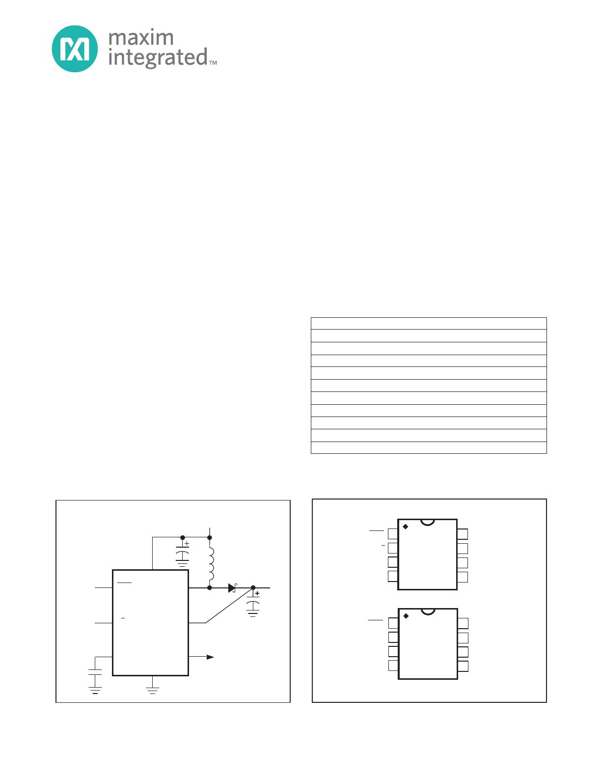
1
2
3
4
8
7
6
5
LX
GND
OUT
LBI
LBO
REF
3/5
SHDN
MAX756
DIP/SO
TOP VIEW
1
2
3
4
8
7
6
5
LX
GND
OUT
LBI
LBO
REF
FB
SHDN
MAX757
DIP/SO
_________________Pin Configurations
MAX756
SHDN
1
3/5
2
REF
3
LBI
5
LX
7
150μF
GND
OUT
6
INPUT
2V to V
OUT
1N5817
OUTPUT
5V at 200mA
or
3.3V at 300mA
100μF
LBO
4
8
0.1μF
22μH
LOW-BATTERY
DETECTOR OUTPUT
__________Typical Operating Circuit
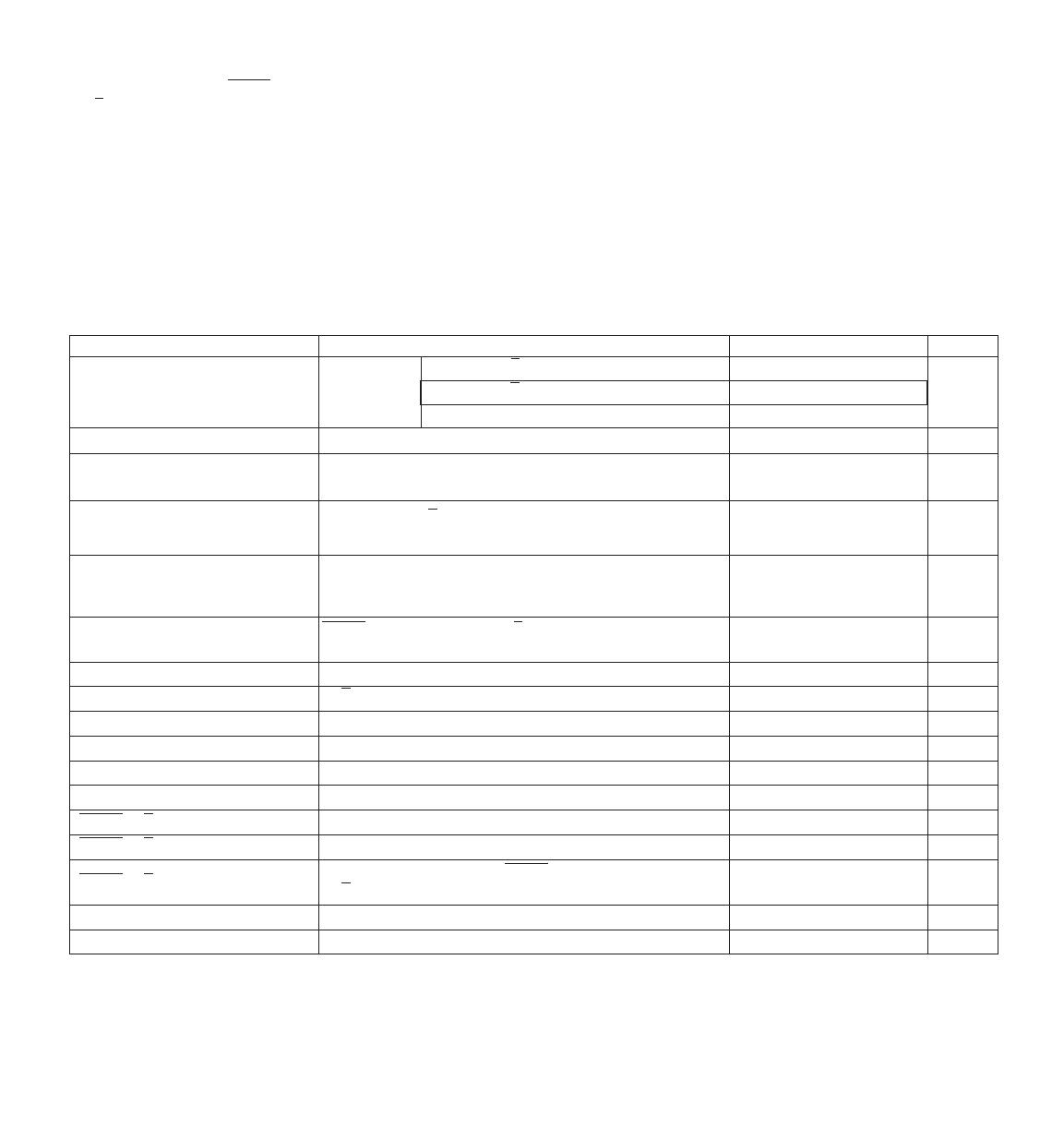
PART TEMP. RANGE PIN-PACKAGE
MAX756CPA
0°C to +70°C 8 Plastic DIP
MAX756CSA 0°C to +70°C 8 SO
MAX756C/D 0°C to +70°C Dice*
MAX756EPA -40°C to +85°C 8 Plastic DIP
MAX756ESA -40°C to +85°C 8 SO
MAX757CPA
0°C to +70°C 8 Plastic DIP
MAX757CSA 0°C to +70°C 8 SO
MAX757C/D 0°C to +70°C Dice*
MAX757EPA -40°C to +85°C 8 Plastic DIP
MAX757ESA -40°C to +85°C 8 SO
3.3V/5V/Adjustable-Output,
Step-Up DC-DC Converters
19-0113; Rev. 2; 1/95
_______________General Description
The MAX756/MAX757 are CMOS step-up DC-DC switch-
ing regulators for small, low input voltage or battery-pow-
ered systems. The MAX756 accepts a positive input
voltage down to 0.7V and converts it to a higher pin-
selectable output voltage of 3.3V or 5V. The MAX757 is
an adjustable version that accepts an input voltage down
to 0.7V and generates a higher adjustable output voltage
in the range from 2.7V to 5.5V. Typical full-load efficiencies
for the MAX756/MAX757 are greater than 87%.
The MAX756/MAX757 provide three improvements over
previous devices. Physical size is reduced—the high
switching frequencies (up to 0.5MHz) made possible by
MOSFET power transistors allow for tiny (<5mm diameter)
surface-mount magnetics. Efficiency is improved to 87%
(10% better than with low-voltage regulators fabricated in
bipolar technology). Supply current is reduced to 60µA
by CMOS construction and a unique constant-off-time
pulse-frequency modulation control scheme.
________________________Applications
3.3V to 5V Step-Up Conversion
Palmtop Computers
Portable Data-Collection Equipment
Personal Data Communicators/Computers
Medical Instrumentation
2-Cell & 3-Cell Battery-Operated Equipment
Glucose Meters
____________________________Features
♦ Operates Down to 0.7V Input Supply Voltage
♦ 87% Efficiency at 200mA
♦ 60µA Quiescent Current
♦ 20µA Shutdown Mode with Active Reference and
LBI Detector
♦ 500kHz Maximum Switching Frequency
♦ ±1.5% Reference Tolerance Over Temperature
♦ Low-Battery Detector (LBI/LBO)
♦ 8-Pin DIP and SO Packages
______________Ordering Information
* Dice are tested at T
A
= +25°C only.