13/19
BDxxIA5WEFJ
Datasheet
TSZ02201-0R6R0A600440-1-2
© 2012 ROHM Co., Ltd. All rights reserved.
www.rohm.com
TSZ2211115001
21.Dec.2012 Rev.002
Input-to-Output Capacitor
It is recommended that a capacitor (over 1uF) is placed near pins between the input pin and GND as well as the output pin
and GND. A capacitor, between input pin and GND, is valid when the power supply impedance is high or trace is long. Also,
as for the capacitor between the output pin and GND, the greater the capacitance, the more sustainable the line regulation
will be and the capacitor will make improvements of characteristics depending on the load. However, please check the
actual functionality of this part by mounting it on a board for the actual application. Ceramic capacitors usually have different,
thermal and equivalent series resistance characteristics, and moreover capacitance decreases gradually in use.
For additional details, please check with the manufacturer, and select the best ceramic capacitor for your application.
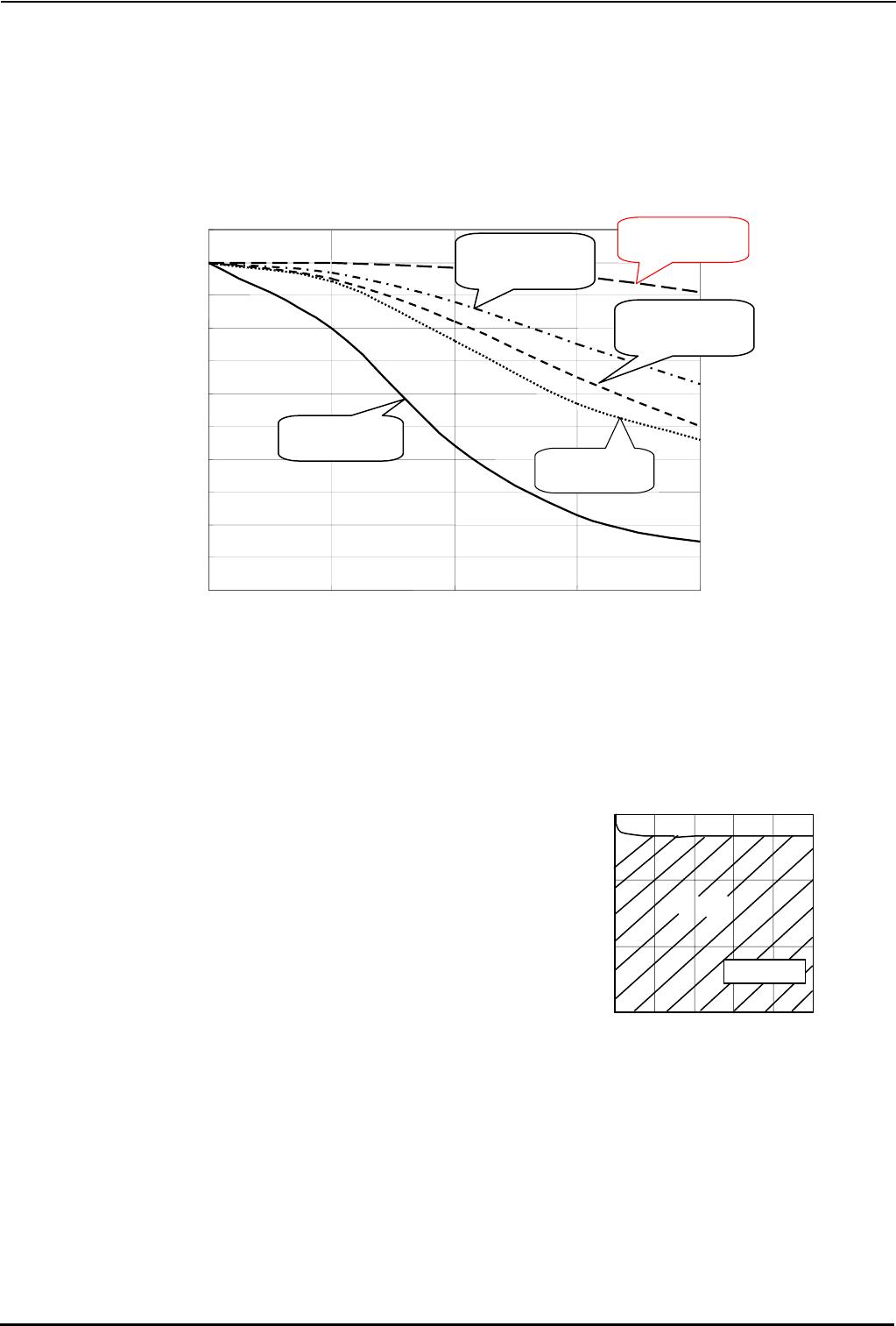
Equivalent Series Resistance ESR (Output Capacitor)
To prevent oscillations, please attach a capacitor between
V
O
and GND. Capacitors usually have ESR (Equivalent
Series Resistance). Operation will be stable in the ESR-I
O
range shown to the right. Ceramic, tantalum and
electrolytic Capacitors have different ESR values, so
please ensure that you are using a capacitor that operates
in the stable operating region shown on the right. Finally,
please evaluate in the actual application.
ESR – I
O
characteristics
DC Bias Voltage [V]
Ceramic capacitor capacity – DC bias characteristics
(Characteristics example)
-100
-90
-80
-70
-60
-50
-40
-30
-20
-10
0
10
0 1 2 3 4
Rated Voltage10V
B1 characteristics
Rated Voltage4V
X6S characteristics
Capacitance Change [%]
Rated Voltage:10V
F characteristics
Rated Voltage6.3V
B characteristics
B characteristics
Rated Voltage10V
0.01
0.10
1.00
10.00
0 0.1 0.2 0.3 0.4 0.5
Io [A]
ESR [Ω]
Safety area
C
O
=1uF
14/19
BDxxIA5WEFJ
Datasheet
TSZ02201-0R6R0A600440-1-2
© 2012 ROHM Co., Ltd. All rights reserved.
www.rohm.com
TSZ2211115001
21.Dec.2012 Rev.002
Evaluation Board Circuit
Evaluation Board Parts List
Designation Value Part No. Company Designation Value Part No. Company
R1
16kΩ
MCR01PZPZF1602 ROHM C4
R2
7.5kΩ
MCR01PZPZF7501 ROHM C5 1μF CM105B105K16A KYOCERA
R3
C6
R4
C7
R5
C8
R6
C9
C1 1μF CM105B105K16A KYOCERA C10
C2
U1
BD00IA5WEFJ ROHM
C3
U2
Board Layout
PCB layout considerations:
Input capacitor C
IN
connected to V
CC
(Vin) should be placed as close to V
CC
(V
IN
) pin as possible.
Output capacitor C
OUT
also should be placed as close to IC pin as possible. In case the part is connected to inner layer
GND plane, please use several through holes.
FB pin has comparatively high impedance and can be affected by noise, so stray capacitance should be as small as
possible. Please take care of this during layout.
Please make GND pattern wide enough to handle thermal dissipation.
For output voltage setting
Output voltage can be set by FB pin voltage (0.800V typ.) and external resistance R1, R2.
(The use of resistors with R1+R2=1k to 90k is recommended)
V
O
EN
GND
(
V
CC
V
IN
)
C
IN
R1
R2
C
OUT
N.C
GND
FB
N.C
N.C.
V
O
2
Vo
C7
3
4
7
5
U1
8
C1
C2
C3
R1
R2
C6
C5
1
V
CC
6
EN
GND
SW1
EN
FIN
Vcc
V
O
= V
FB
×
R1+R2
R2
15/19
BDxxIA5WEFJ
Datasheet
TSZ02201-0R6R0A600440-1-2
© 2012 ROHM Co., Ltd. All rights reserved.
www.rohm.com
TSZ2211115001
21.Dec.2012 Rev.002
I/O Equivalent Circuits (Output Voltage Vairable type)
8pin(V
CC
) / 1pin(V
O
) 2pin(FB) 5pin(EN)
I/O Equivalent Circuits (Output Voltage Fixed type)
2pin(FB)
8pin(V
CC
)
1pn(V
O
)
5pin(EN)
520kΩ
480kΩ
8pin(V
CC
) / 1pin(V
O
) 2pin(V
O_S
) 5pin(EN)
8pin(V
CC
)
1pin(V
O
)
2pin(V
O_S
)
5pin(EN)
520kΩ
480kΩ

BD30IA5WEFJ-E2

Mfr. #:
Manufacturer:
Description:
LDO Voltage Controllers LDO Reg Pos 3.0V 0.5A
Lifecycle:
New from this manufacturer.
Delivery:
DHL FedEx Ups TNT EMS
Payment:
T/T Paypal Visa MoneyGram Western Union