LTC3400/LTC3400B
5
3400fa
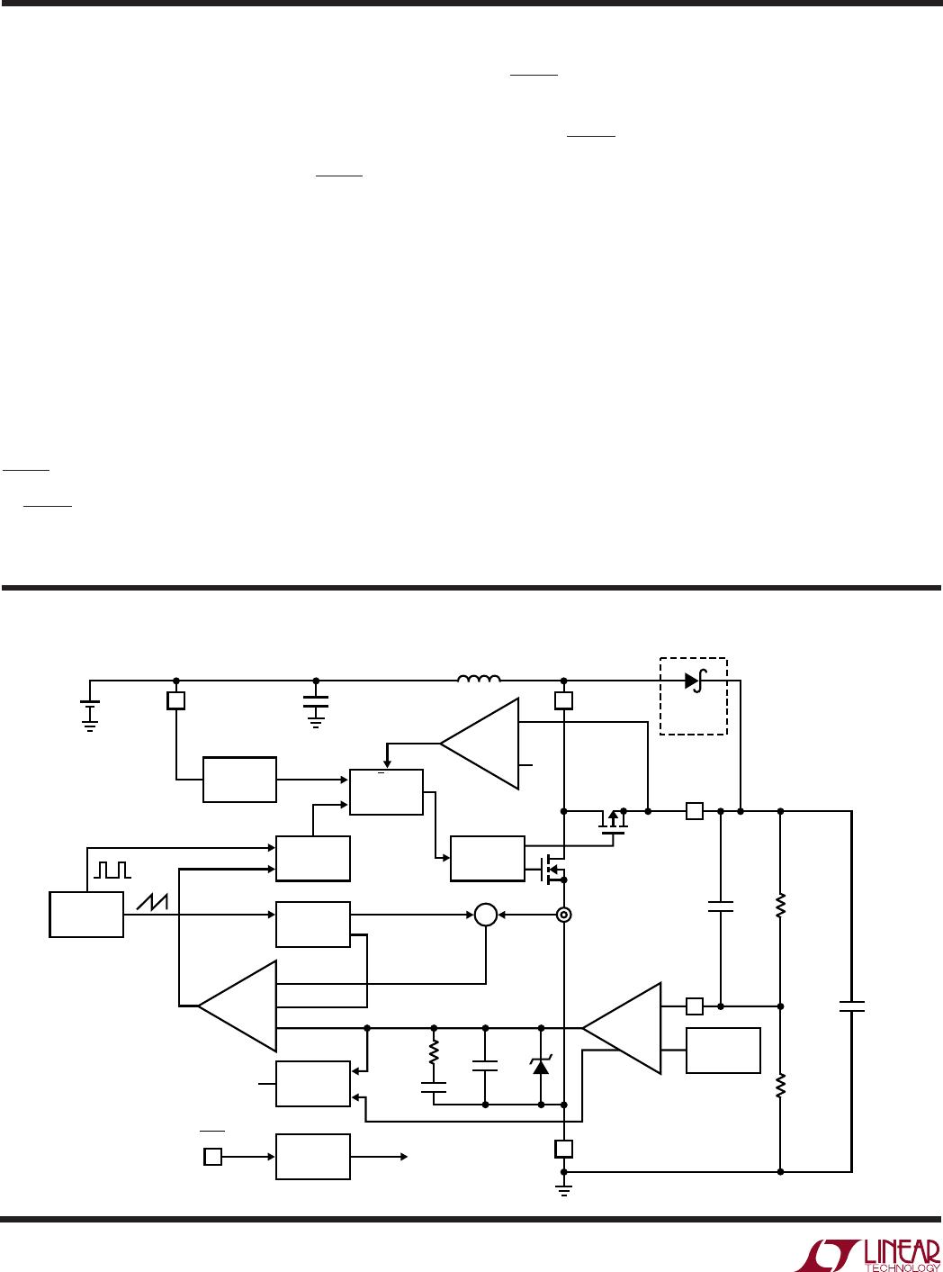
OPERATIO
U
The LTC3400/LTC3400B are 1.2MHz, synchronous boost
converters housed in a 6-lead ThinSOT package. Able to
operate from an input voltage below 1V, the devices
feature fixed frequency, current mode PWM control for
exceptional line and load regulation. With its low R
DS(ON)
and gate charge internal MOSFET switches, the devices
maintain high efficiency over a wide range of load current.
Detailed descriptions of the three distinct operating modes
follow. Operation can be best understood by referring to
the Block Diagram.
Low Voltage Start-Up
The LTC3400/LTC3400B will start up at a typical V
IN
volt-
age of 0.85V or higher. The low voltage start-up circuitry
controls the internal NMOS switch up to a maximum peak
inductor current of 850mA (typ), with an approximate
1.5µs off-time during start-up, allowing the devices to
start up into an output load. Once V
OUT
exceeds 2.3V, the
start-up circuitry is disabled and normal fixed frequency
PWM operation is initiated. In this mode, the LTC3400/
LTC3400B operate independent of V
IN
, allowing extended
operating time as the battery can droop to several tenths
of a volt without affecting output voltage regulation. The
limiting factor for the application becomes the ability of the
battery to supply sufficient energy to the output.
Low Noise Fixed Frequency Operation
Oscillator: The frequency of operation is internally set to
1.2MHz.
Error Amp: The error amplifier is an internally compensated
transconductance type (current output) with a transconduc-
tance (g
m
) = 33 microsiemens. The internal 1.23V reference
voltage is compared to the voltage at the FB pin to generate
an error signal at the output of the error amplifier. A volt-
age divider from V
OUT
to ground programs the output
voltage via FB from 2.5V to 5V using the equation:
V
OUT
= 1.23V • [1 + (R1/R2)]
Current Sensing: A signal representing NMOS switch
current is summed with the slope compensator. The
summed signal is compared to the error amplifier output
to provide a peak current control command for the PWM.
Peak switch current is limited to approximately 850mA
independent of input or output voltage. The current signal
is blanked for 40ns to enhance noise rejection.
Zero Current Comparator: The zero current comparator
monitors the inductor current to the output and shuts off
the synchronous rectifier once this current reduces to ap-
proximately 20mA. This prevents the inductor current from
reversing in polarity improving efficiency at light loads.
Antiringing Control: The antiringing control circuitry pre-
vents high frequency ringing of the SW pin as the inductor
current goes to zero by damping the resonant circuit
formed by L and C
SW
(capacitance on SW pin).
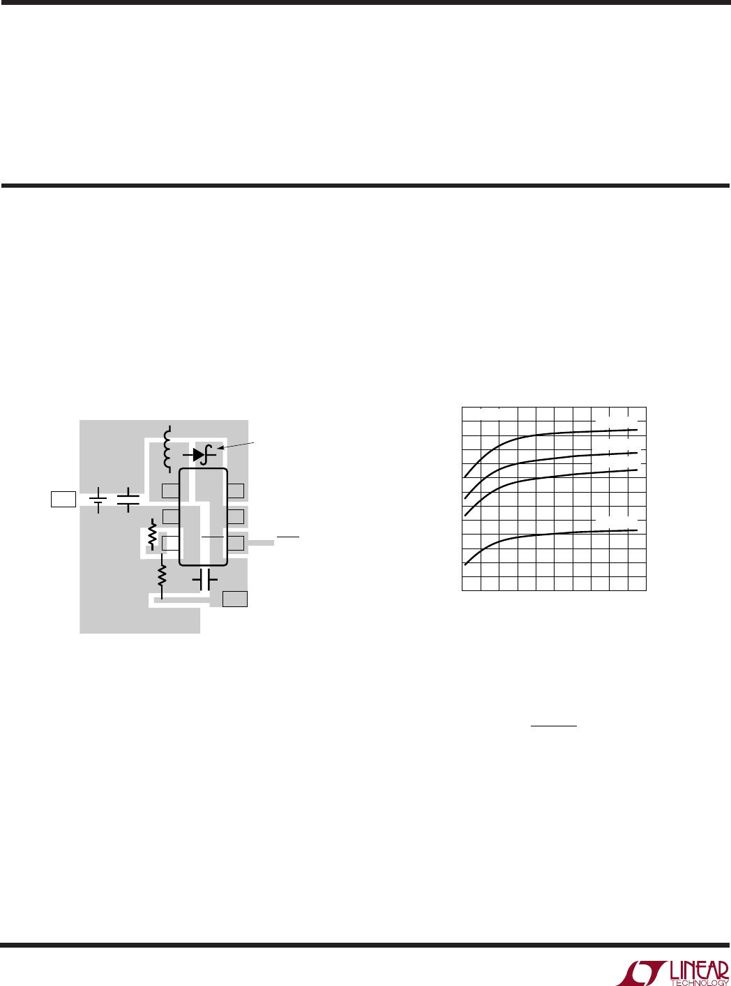
Burst Mode Operation
Portable devices frequently spend extended time in low
power or standby mode, only switching to high power
drain when specific functions are enabled. In order to
improve battery life in these types of products, high power
converter efficiency needs to be maintained over a wide
output power range. In addition to its high efficiency at
moderate and heavy loads, the LTC3400 includes auto-
matic Burst Mode operation that improves efficiency of
the power converter at light loads. Burst mode operation
is initiated if the output load current falls below an
internally programmed threshold (see Typical Perfor-
mance graph, Output Load Burst Mode Threshold vs V
IN
).
Once initiated, the Burst Mode operation circuitry shuts
down most of the device, only keeping alive the circuitry
required to monitor the output voltage. This is referred to
as the sleep state. In sleep, the LTC3400 draws only 19µA
from the output capacitor, greatly en
hancing efficiency.
When the output voltage has drooped approximately 1%
from nominal, the LTC3400 wakes up and commences
normal PWM operation. The output capacitor recharges
and causes the LTC3400 to reenter sleep if the output load
remains less than the sleep threshold. The frequency of
this intermittent PWM or burst operation is proportional to
load current; that is, as the load current drops further
below the burst threshold, the LTC3400 turns on less
frequently. When the load current increases above the