Ver.5
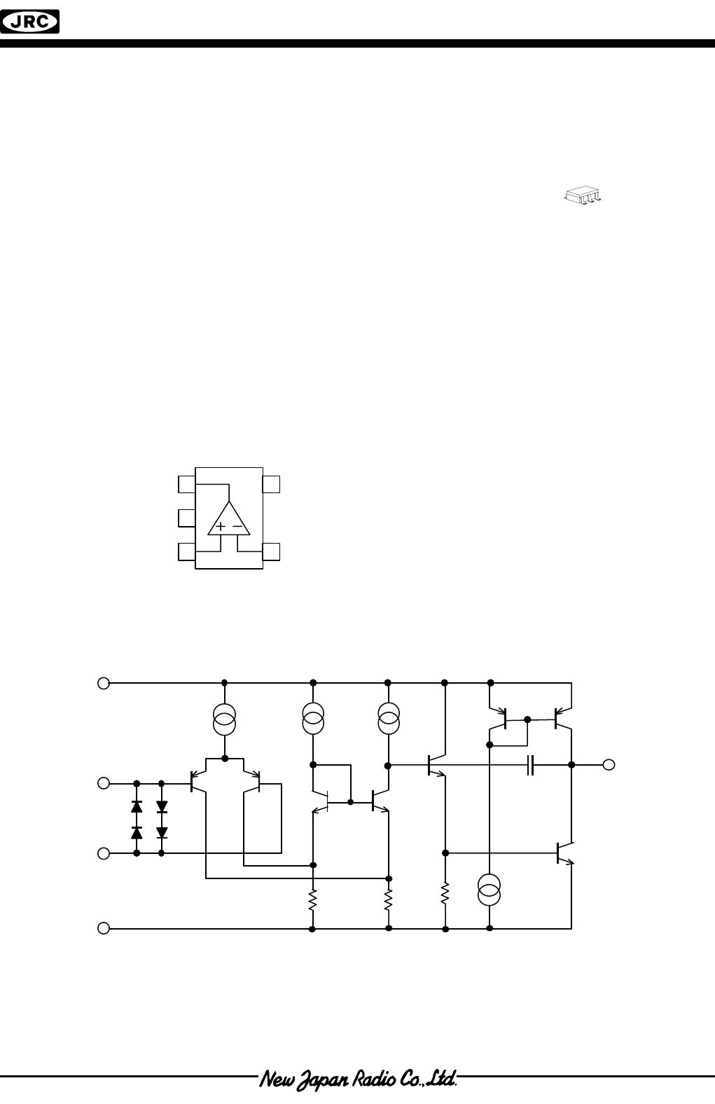
NJM2716
-
-
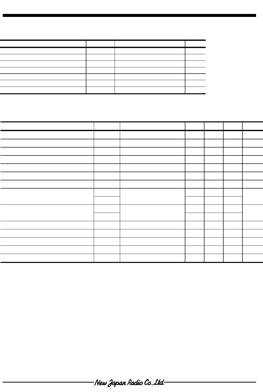
g ABSOLUTE MAXIMUM RATINGS (Ta=25°C)
PARAMETER SYMBOL RATINGS UNIT
Supply Voltage V
+
15.0 V
Power Dissipation P
D
200 mW
Differential Input Voltage V
ID
±3
V
Input Voltage V
IC
-0.3 to +15 (note) V
Output Sink Current I
SINK
10 mA
Operating Temperature Range Topr -40 to +85
°C
Storage Temperature Range Tstg -40 to +125
°C
(note) When supply voltage is less than 15V, the absolute maximum
input voltage is equal to the supply voltage.
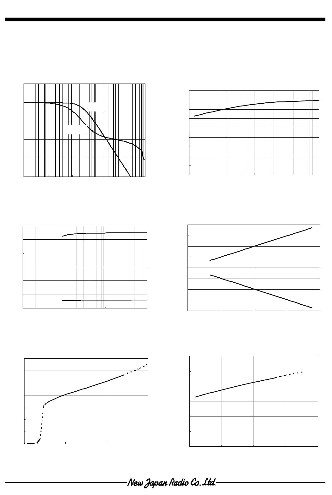
g ELECTRICAL CHARACTERISTICS ( V
+
=5V,Ta=25°C)
PARAMETER SYMBOL TEST CONDITION MIN. TYP. MAX. UNIT
Input Offset Voltage V
IO
Rs=0Ω
- 1 10 mV
Input Offset Current I
IO
- 0.2 0.5
µA
Input Bias Current I
B
- 1 2.5
µA
Voltage Gain A
V
R
L
≥10kΩ
60 75 - dB
Input Common Mode Voltage Range V
ICM
0 to 3.8 - - V
Common Mode Rejection Ratio CMR 45 80 - dB
Supply Voltage Rejection Ratio SVR 50 75 - dB
V
OM
+
1 4.3 4.5 -
Maximum Output Voltage1
V
OM
-
1
R
L
=4kΩ to GND
- 0.05 0.1
V
V
OM
+
2 4.5 4.7 -
Maximum Output Voltage 2
V
OM
-
2
R
L
=4kΩ to 2.5V
- 0.1 0.5
V
Output Source Current I
SOURCE
1 2.5 - mA
Output Sink Current I
SINK
2.5 5 - mA
Operating Current Icc
R
L
=∞
- 4.2 5.5 mA
Slew Rate SR - 40 -
V/µs
Unity Gain Bandwidth f
T
- 30 - MHz