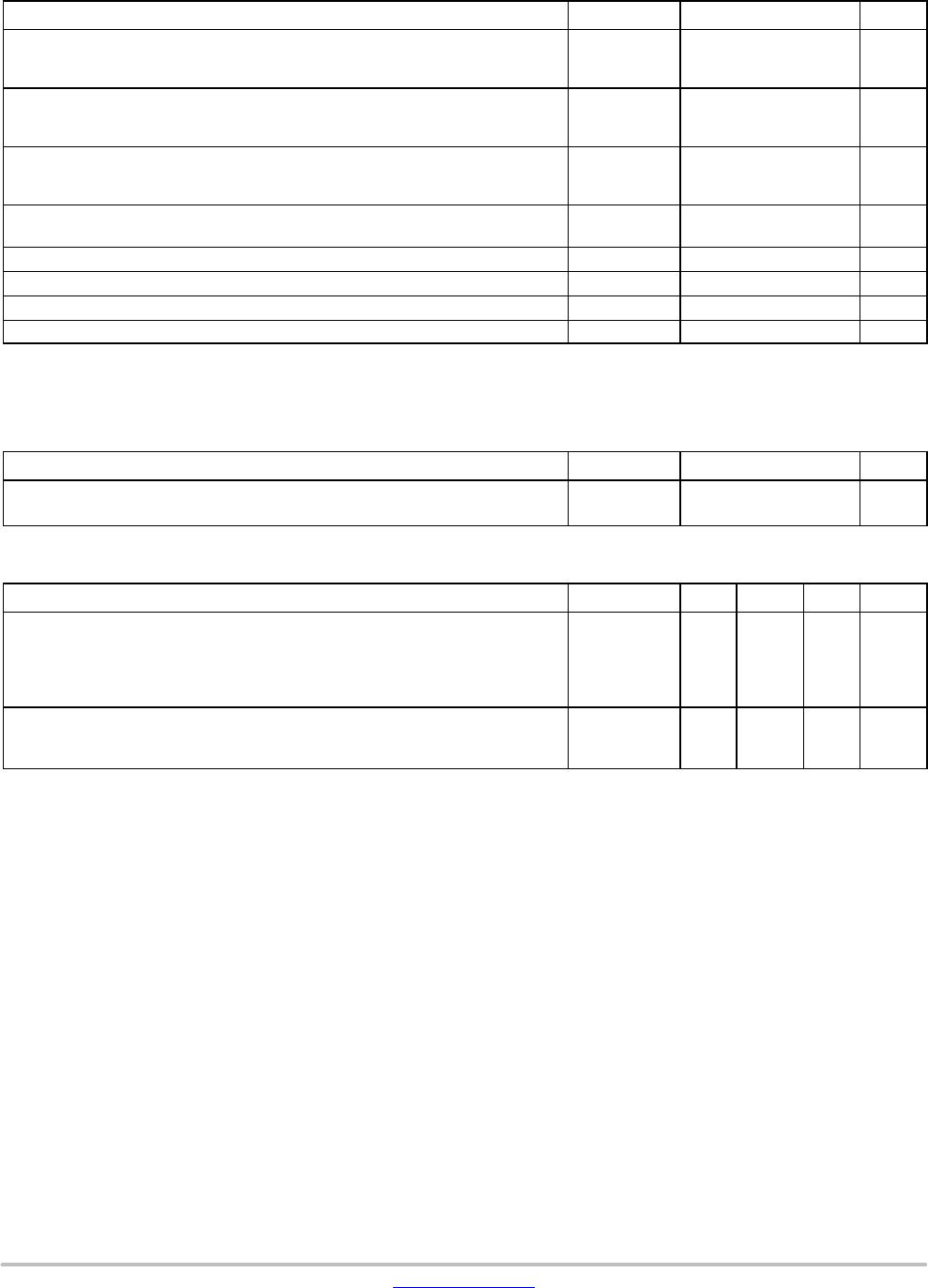
MBR16100CTG

© Semiconductor Components Industries, LLC, 2015
January, 2015 − Rev. 6
1 Publication Order Number:
MBR16100CT/D
MBR16100CTG
Switch-mode
Power Rectifier
Features and Benefits
Low Forward Voltage
Low Power Loss/High Efficiency
High Surge Capacity
175°C Operating Junction Temperature
Low Stored Charge Majority Carrier Conduction
16 A Total (8.0 A Per Diode Leg)
This Device is Pb−Free and is RoHS Compliant*
Applications
Power Supply − Output Rectification
Power Management
Instrumentation
Mechanical Characteristics
Case: Epoxy, Molded
Epoxy Meets UL 94 V−0 @ 0.125 in
Weight: 1.9 Grams (Approximately)
Finish: All External Surfaces Corrosion Resistant and Terminal
Leads are Readily Solderable
Lead Temperature for Soldering Purposes:
260°C Max. for 10 Seconds
ESD Rating: Human Body Model = 3B
Machine Model = C
*For additional information on our Pb−Free strategy and soldering details, please
download the ON Semiconductor Soldering and Mounting Techniques
Reference Manual, SOLDERRM/D.
Device Package Shipping
ORDERING INFORMATION
SCHOTTKY BARRIER
RECTIFIER
16 AMPERES, 100 VOLTS
1
3
2, 4
www.onsemi.com
MBR16100CTG TO−220
(Pb−Free)
50 Units/Rail
TO−220
CASE 221A
STYLE 6
3
4
1
2
MARKING
DIAGRAM
A = Assembly Location
Y = Year
WW = Work Week
B16100 = Device Code
G = Pb−Free Package
AKA = Diode Polarity
AYWW
B16100G
AKA
MBR16100CTG
www.onsemi.com
2
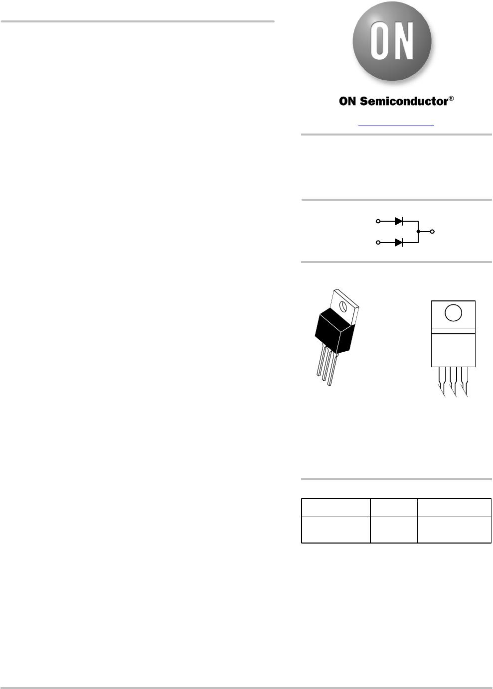
MAXIMUM RATINGS (Per Diode Leg)
Rating
Symbol Value Unit
Peak Repetitive Reverse Voltage
Working Peak Reverse Voltage
DC Blocking Voltage
V
RRM
V
RWM
V
R
100 V
Average Rectified Forward Current
(T
C
= 166°C) Per Diode
Per Device
I
F(AV)
8.0
16
A
Peak Repetitive Forward Current
(Square Wave, 20 kHz)
T
C
= 165°C
I
FRM
16 A
Non-repetitive Peak Surge Current
(Surge applied at rated load conditions half-wave, single phase, 60 Hz)
I
FSM
150 A
Peak Repetitive Reverse Surge Current (2.0 ms, 1.0 kHz)
I
RRM
0.5 A
Operating Junction Temperature (Note 1) T
J
*65 to +175 °C
Storage Temperature T
stg
*65 to +175 °C
Voltage Rate of Change (Rated V
R
) dv/dt 10,000
V/ms
Stresses exceeding those listed in the Maximum Ratings table may damage the device. If any of these limits are exceeded, device functionality
should not be assumed, damage may occur and reliability may be affected.
1. The heat generated must be less than the thermal conductivity from Junction−to−Ambient: dP
D
/dT
J
< 1/R
q
JA
.
THERMAL CHARACTERISTICS
Characteristic Symbol Value Unit
Maximum Thermal Resistance, Junction−to−Case (Min. Pad)
Junction−to−Ambient (Min. Pad)
R
q
JC
R
q
JA
2.0
60
°C/W
ELECTRICAL CHARACTERISTICS (Per Diode Leg)
Characteristic
Symbol Min Typical Max Unit
Maximum Instantaneous Forward Voltage (Note 2)
(i
F
= 8.0 A, T
J
= 125°C)
(i
F
= 8.0 A, T
J
= 25°C)
(i
F
= 16 A, T
J
= 125°C)
(i
F
= 16 A, T
J
= 25°C)
v
F
0.56
0.68
0.67
0.79
0.60
0.74
0.69
0.84
V
Maximum Instantaneous Reverse Current (Note 2)
(Rated dc Voltage, T
J
= 125°C)
(Rated dc Voltage, T
J
= 25°C)
i
R
0.95
0.0013
5.0
0.1
mA
Product parametric performance is indicated in the Electrical Characteristics for the listed test conditions, unless otherwise noted. Product
performance may not be indicated by the Electrical Characteristics if operated under different conditions.
2. Pulse Test: Pulse Width = 300 ms, Duty Cycle 2%.
MBR16100CTG
www.onsemi.com
3
Figure 1. Typical Forward Voltage Per Diode Figure 2. Maximum Forward Voltage Per Diode
0.60
V
F
, INSTANTANEOUS FORWARD VOLTAGE (VOLTS)
100
10
0.2 0.4 0.8
1
0.1
1
T
J
= 25°C
175°C
125°C
75°C
0.50.1 0.3 0.7 0.9
i
F
, INSTANTANEOUS FORWARD
VOLTAGE (AMPS)
0.60
V
F
, INSTANTANEOUS FORWARD VOLTAGE (VOLTS)
100
10
0.2 0.4 0.8
1
0.1
1
T
J
= 25°C
175°C
125°C
75°C
0.50.1 0.3 0.7 0.9
I
F
, INSTANTANEOUS FORWARD
CURRENT (AMPS)
Figure 3. Typical Reverse Current Per Diode Figure 4. Typical Capacitance Per Diode
0
V
R
, REVERSE VOLTAGE (VOLTS)
10 20 30 40 100
Figure 5. Current Derating, Case Per Leg Figure 6. Current Derating, Ambient Per Leg
50 60 70 80 90
I
R
, REVERSE CURRENT (AMPS)
T
J
= 25°C
175°C
125°C
75°C
0
V
R
, REVERSE VOLTAGE (VOLTS)
10 20 30 40 10
0
50 60 70 80 90
I
R
, REVERSE CURRENT (AMPS)
T
J
= 25°C
175°C
125°C
75°C
I , AVERAGE FORWARD CURRENT (AMPS)
F (AV)
T
A
, AMBIENT TEMPERATURE (°C)
05025 75
2.0
4.0
6.0
8.0
10
T
C
, CASE TEMPERATURE (C°)
180
14
4.0
0
dc
SQUARE WAVE
145 155 160
I , AVERAGE FORWARD CURRENT (AMPS)
F (AV)
2.0
12
16
6.0
8.0
10
12
14
16
140
150
0
100 125 150 175
SQUARE WAVE
RATED VOLTAGE APPLIED
R
q
JA
= 16° C/W
dc
R
q
JA
= 60° C/W
(NO HEATSINK)
170 175
165
dc
1E−1
1E−2
1E−3
1E−6
1E−7
1E−5
1E−4
1E−1
1E−2
1E−3
1E−6
1E−7
1E−5
1E−4

MBR16100CTG

Mfr. #:
Manufacturer:
ON Semiconductor
Description:
Schottky Diodes & Rectifiers 16A 100V
Lifecycle:
New from this manufacturer.
Delivery:
DHL FedEx Ups TNT EMS
Payment:
T/T Paypal Visa MoneyGram Western Union

Products related to this Datasheet