© Semiconductor Components Industries, LLC, 2015
January, 2015 − Rev. 1
1 Publication Order Number:
TCP−3112H/D
TCP-3112H
1.2 pF Passive Tunable
Integrated Circuits (PTIC)
Introduction
ON Semiconductor’s PTICs have excellent RF performance and
power consumption, making them suitable for any mobile handset or
radio application. The fundamental building block of our PTIC
product line is a tunable material called ParaScant, based on Barium
Strontium Titanate (BST). PTICs have the ability to change their
capacitance from a supplied bias voltage generated by the Control IC.
The 1.2 pF PTICs are available as wafer-level chip scale packages
(WLCSP).
Key Features
• High Tuning Range and Operation up to 20 V
• Usable Frequency Range: from 700 MHz to 2.7 GHz
• High Quality Factor (Q) for Low Loss
• High Power Handling Capability
• Compatible with PTIC Control IC TCC-10x, 20x
• WLCSP Package: 0.652 x 0.834 x 0.285 mm (8 bump)
• These devices are Pb−Free and RoHS Compliant
Typical Applications
• Multi-band, Multi-standard, Advanced and Simple Mobile Phones
• Tunable Antenna Matching Networks
• Tunable RF Filters
• Active Antennas
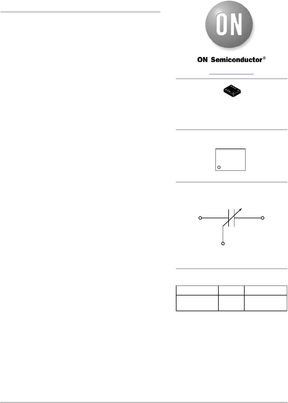
MARKING DIAGRAM
Device Package Shipping
†
ORDERING INFORMATION
www.
onsemi.com
TCP−3112H−DT WLCSP8
(Pb−Free)
4000 Units /
7” Tape & Reel
WLCSP8
0.83x0.65
CASE 567KF
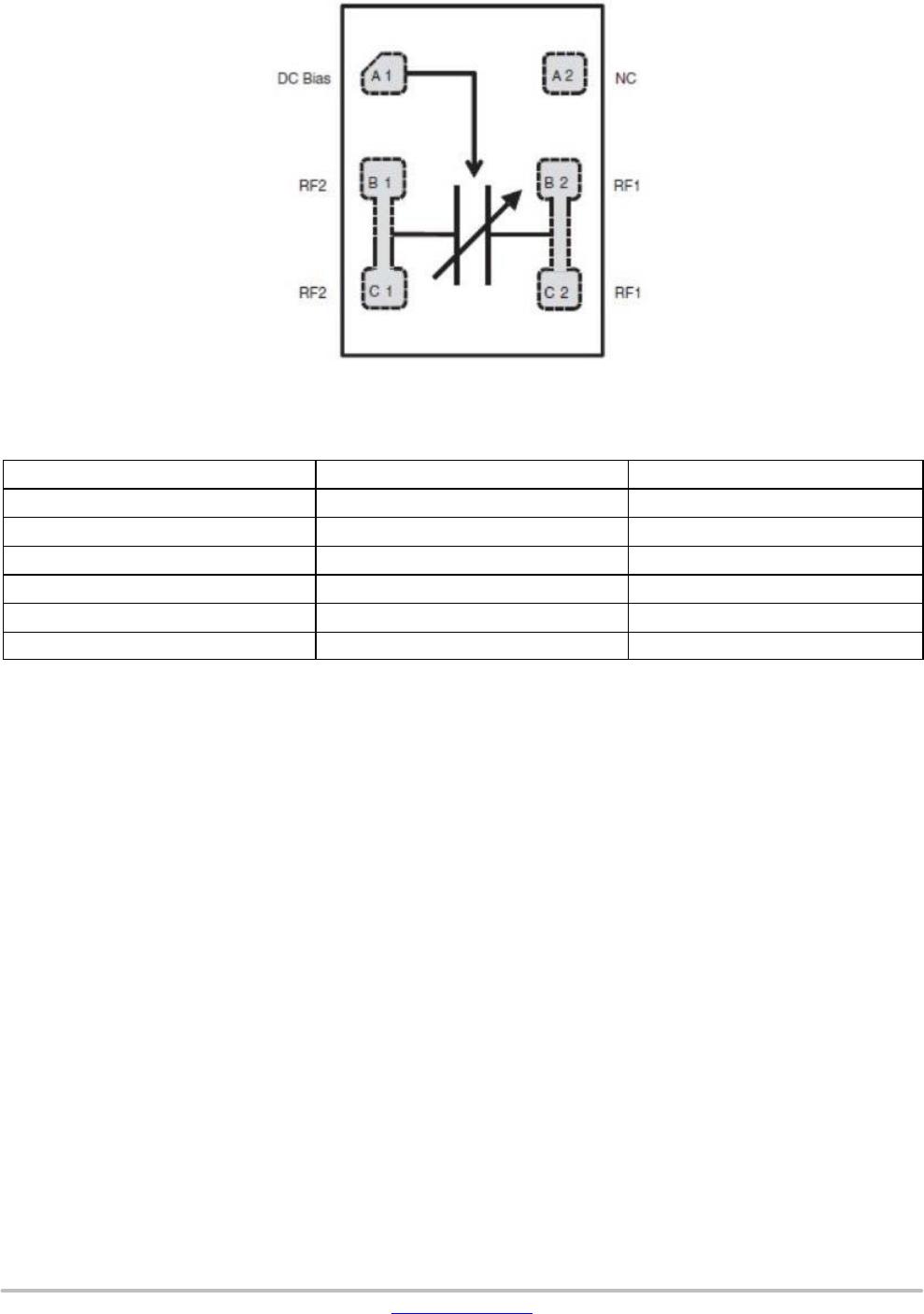
FUNCTIONAL BLOCK DIAGRAM
PTIC Functional Block Diagram
PTIC
Bias
RF1 RF2
†For information on tape and reel specifications,
including part orientation and tape sizes, please
refer to our Tape and Reel Packaging Specification
Brochure, BRD8011/D.