LTC1864/LTC1865
20
18645fb
APPLICATIONS INFORMATION
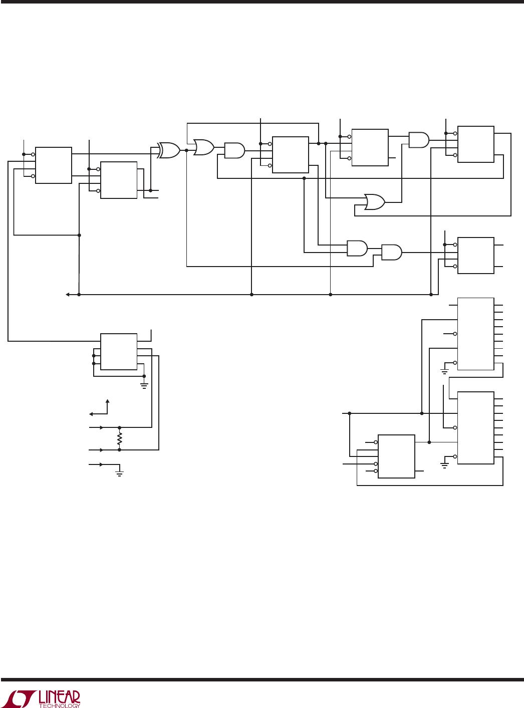
Transmit LTC1864 Data Over Modular Telephone Wire
Using Simple Transmitter/Receiver
Figure 6 shows a simple Manchester encoder and dif-
ferential transmitter suitable for use with the LTC1864.
This circuit allows transmission of data over inexpensive
telephone wire. This is useful for measuring a remote
sensor, particularly when the cost of preserving the analog
signal over a long distance is high.
Manchester encoding is a clock signal that is modulated
by exclusive ORing with the data signal. The resulting
signal contains both clock and data information and has
an average duty cycle of 50%, that also allows transformer
coupling. In practice, generating a Manchester encoded
signal with an XOR gate will often produce glitches due
to the skew between data and clock transitions. The D
fl ip-fl ops in this encoder retime the clock and data such
that the respective edges are closely aligned, effectively
suppressing glitches. The retimed data and clock are then
XORed to produce the Manchester encoded data, which
is interfaced to telephone wire with an LTC1485 RS485
transceiver.
In order to synchronize to incoming data, the receiver
needs a sequence to indicate the start of a data word. The
transmitter schematic shows logic that will produce 31
zeros, a start bit, followed by the 16 data bits (one sample
every 48 clock cycles) at a clock frequency of 1MHz set by
the LTC1799 oscillator. Sending at least 18 zeros before
each start bit ensures that if synchronization is lost, the
receiver can resynchronize to a start bit under all condi-
tions. The serial to parallel converter shown in Figure 7
requires 18 zeros to avoid triggering on data bits.
The Manchester receiver shown in Figure 7 was adopted
from Xilinx application note 17-30 and would typically be
implemented in an FPGA. The decoder clock frequency is
nominally 8 times the transmit clock frequency and is very
tolerant of frequency errors. The outputs of the decoder
are data and a strobe that indicates a valid data bit. The
data can be deserialized using shift registers as shown.
The start bit resets the J-K/fl ip-fl op on its way into the
fi rst shift register. When it appears at the QH
IN
output of
the second shift register, it sets the fl ip-fl op that loads the
parallel data into the output register.
With AC family CMOS logic at 5V the receiver clock fre-
quency is limited to 20MHz; the corresponding transmitter
clock frequency is 2.5MHz. If the receiver is implemented
in an FPGA that can be clocked at 160MHz, the LTC1864
can be clocked at its rated clock frequency of 20MHz.