PTFA180701E-V4-R250

PTFA180701E
PTFA180701F
All published data at T
CASE
= 25°C unless otherwise indicated
ESD: Electrostatic discharge sensitive device—observe handling precautions!
Data Sheet 1 of 11 Rev. 03.1, 2009-02-20
Description
The PTFA180701E and PTFA180701F are 70-watt LDMOS FETs designed
for GSM and GSM EDGE power amplifier applications in the 1805 MHz to
1880 MHz band. Features include input and output matching, and thermally-
enhanced packages with slotted or earless flanges. Manufactured with
Infineon's advanced LDMOS process, these devices provide excellent
thermal performance and superior reliability.
Features
Thermally-enhanced packages, Pb-free and
RoHS-compliant
Broadband internal matching
Typical EDGE performance
- Average output power = 44 dBm
- Gain = 16.5 dB
- Efficiency = 40.5%
- EVM = 2.0%
Typical CW performance
- Output power at P–1dB = 72 W
- Gain = 15.5 dB
- Efficiency = 59%
Integrated ESD protection: Human Body
Model, Class 2 (minimum)
Excellent thermal stability, low HCI drift
Capable of handling 10:1 VSWR @ 28 V,
70 W (CW) output power
RF Characteristics
EDGE Measurements (not subject to production test—verified by design/characterization in Infineon test fixture)
V
DD
= 28 V, I
DQ
= 550 mA, P
OUT
= 44 dBm, ƒ = 1836.6 MHz
Characteristic Symbol Min Typ Max Unit
Error Vector Magnitude EVM RMS 2.0 %
Modulation Spectrum @ 400 kHz ACPR –62 dBc
@ 600 kHz ACPR –76 dBc
Gain G
ps
16.5 dB
Drain Efficiency η
D
40.5 %
Thermally-Enhanced High Power RF LDMOS FETs
70 W, 1805 – 1880 MHz
*See Infineon distributor for future availability.
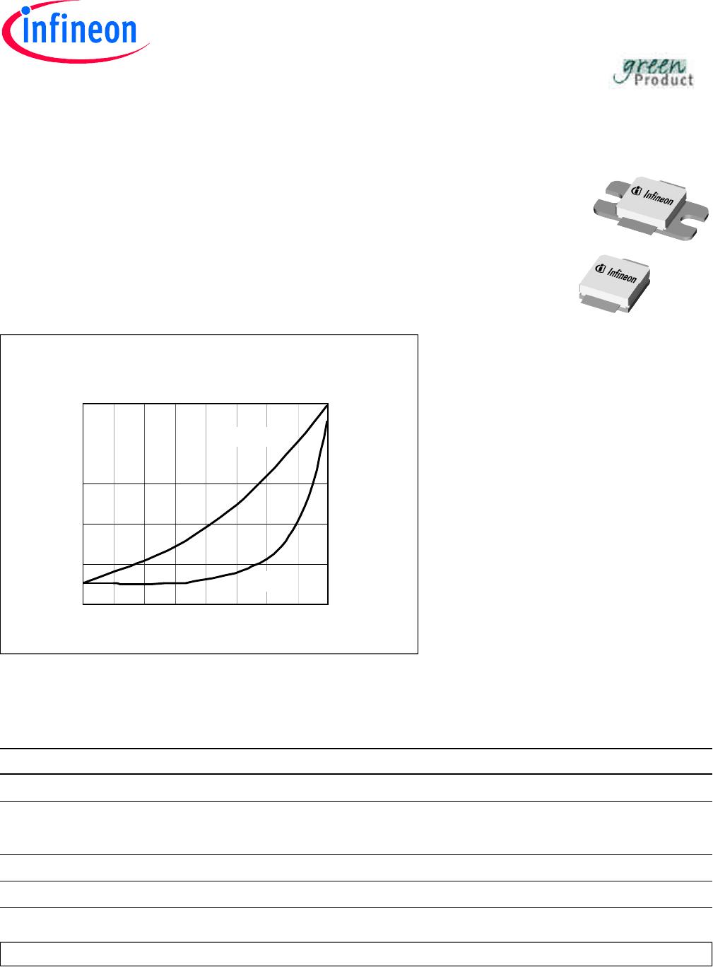
EDGE EVM Performance
V
DD
= 28 V, I
DQ
= 550 mA, ƒ = 1836.6 MHz
0
1
2
3
4
5
30 32 34 36 38 40 42 44 46
Output Power, avg. (dBm)
EVM RMS (avg. %) .
0
10
20
30
40
50
Drain Efficiency (%)
EVM
Efficiency
PTFA180701E
Package H-36265-2
PTFA180701F
Package H-37265-2
PTFA180701E
PTFA180701F
Data Sheet 2 of 11 Rev. 03.1, 2009-02-20
RF Characteristics (cont.)
Two-tone Measurements (tested in Infineon test fixture)
V
DD
= 28 V, I
DQ
= 550 mA, P
OUT
= 60 W PEP, ƒ = 1840 MHz, tone spacing = 1 MHz
Characteristic Symbol Min Typ Max Unit
Gain G
ps
15.5 16.5 dB
Drain Efficiency η
D
44 45 %
Intermodulation Distortion IMD –30 –29 dBc
DC Characteristics
Characteristic Conditions Symbol Min Typ Max Unit
Drain-Source Breakdown Voltage V
GS
= 0 V, I
DS
= 10 mA V
(BR)DSS
65 V
Drain Leakage Current V
DS
= 28 V, V
GS
= 0 V I
DSS
1.0 µA
V
DS
= 63 V, V
GS
= 0 V I
DSS
10.0 µA
On-State Resistance V
GS
= 10 V, V
DS
= 0.1 V R
DS(on)
0.125
Operating Gate Voltage V
DS
= 28 V, I
D
= 550 mA V
GS
2.0 2.5 3.0 V
Gate Leakage Current V
GS
= 10 V, V
DS
= 0 V I
GSS
1.0 µA
Maximum Ratings
Parameter Symbol Value Unit
Drain-Source Voltage V
DSS
65 V
Gate-Source Voltage V
GS
–0.5 to +12 V
Junction Temperature T
J
200 °C
Total Device Dissipation P
D
201 W
Above 25°C derate by 1.15 W/°C
Storage Temperature Range T
STG
–40 to +150 °C
Thermal Resistance (T
CASE
= 70°C, 70 W CW) R
θJC
0.87 °C/W
Ordering Information
Type and Version Package Type Package Description Marking
PTFA180701E V4 H-36265-2 Thermally-enhanced slotted flange, single-ended PTFA180701E
PTFA180701E V4 H-37265-2 Thermally-enhanced earless flange, single-ended PTFA180701F
*See Infineon distributor for future availability.
Data Sheet 3 of 11 Rev. 03.1, 2009-02-20
PTFA180701E
PTFA180701F
Three-Carrier CDMA2000 Performance
V
DD
= 28 V, I
DQ
= 550 mA, ƒ = 1840 MHz
0
10
20
30
40
50
60
30 32 34 36 38 40 42 44 46
Output Power, Avg. (dBm)
Drain Efficiency (%)
-70
-65
-60
-55
-50
-45
-40
Adj. Ch. Power Ratio (dBc)
ALT Up
ACP Up
Efficiency
ACP Low
Edge EVM and Modulation Spectrum
vs. Quiescent Current
V
DD
= 28 V, ƒ = 1836.6 MHz, P
OUT
= 44 dBm
1.0
1.2
1.4
1.6
1.8
2.0
2.2
2.4
2.6
0.40 0.50 0.60 0.70
Quiescent Current (A)
EVM RMS (avg. %) .
-90
-80
-70
-60
-50
-40
-30
-20
-10
Modulation Spectrum (dBc)
EVM
400 kHz
600 kHz
Typical Performance (measurements taken in production test fixture)
Intermodulation Distortion vs. Output Power
V
DD
= 28 V, I
DQ
= 550 mA, ƒ = 1840 MHz,
tone spacing = 1 MHz
-60
-55
-50
-45
-40
-35
-30
-25
30 35 40 45 50
Output Power, PEP (dBm)
IMD (dBc)
0
10
20
30
40
50
60
70
Efficiency (%)
3rd Order
7th
5th
Efficiency
EDGE Modulation Spectrum Performance
V
DD
= 28 V, I
DQ
= 550 mA, ƒ = 1836.6 MHz
-90
-80
-70
-60
-50
-40
30 32 34 36 38 40 42 44 46
Output Power (dBm)
Modulation Spectrum (dBc)
0
10
20
30
40
50
Drain Efficiency (%)
Efficiency
400 kHz
600 kHz

PTFA180701E-V4-R250

Mfr. #:
Manufacturer:
N/A
Description:
IC FET RF LDMOS 70W H-36265-2
Lifecycle:
New from this manufacturer.
Delivery:
DHL FedEx Ups TNT EMS
Payment:
T/T Paypal Visa MoneyGram Western Union