XC18V00 Series In-System-Programmable Configuration PROMs
DS026 (v5.2) January 11, 2008 www.xilinx.com
Product Specification 13
R
X-Ref Target - Figure 8
Figure 8: Configuring Multiple Devices with Identical Patterns in Master/Slave Serial,
Master/Slave SelectMAP, or Master/Slave Parallel Mode
XC18V00
PROM
First
PROM
(PROM 0)
V
CCINT
V
CCO
(2)
TDI
TMS
TCK
GND
D[0:7](3)
CLK
CE
CEO
OE/RESET
CF
TDO
Xilinx FPGA
Master
Serial/SelectMAP
Xilinx FPGA
Slave
Serial/SelectMAP
D[0:7]
(3)
CCLK
DONE
INIT_B (INIT)
PROG_B (PROGRAM)
TDI
TMS
TCK
GND
MODE PINS
(1)
TDO
4.7 kΩ
4.7 kΩ
(1)
V
CCO
(2)
TDI
TMS
TCK
TDO
Notes:
1 For MODE pin connections and DONE pin pullup value, refer to the appropriate FPGA data sheet or user guide.
2 For compatible voltages, refer to the appropriate data sheet.
3 Serial modes do not require the D[1:7], RDWR_B, or CS_B pins to be connected.
4 External oscillator required if CLK is not supplied by an FPGA in Master mode. Refer to the appropriate FPGA data sheet.
D[0:7]
(3)
CCLK
DONE
INIT_B (INIT)
PROG_B (PROGRAM)
TDI
TMS
TCK
GND
XC18V00
PROM
Cascaded
PROM
(PROM 1)
V
CCINT
V
CCO
(2)
TDI
TMS
TCK
GND
D[0:7](3)
CLK
CE
CEO
OE/RESET
CF
TDO
MODE PINS
(1)
TDO
DS026_17_111207
RDWR_B
(3)
CS_B
(3)
RDWR_B
(3)
CS_B
(3)
V
CCO
V
CCINT
V
CCO
V
CCINT
External
(4)
Oscillator
8 8
XC18V00 Series In-System-Programmable Configuration PROMs
DS026 (v5.2) January 11, 2008 www.xilinx.com
Product Specification 14
R
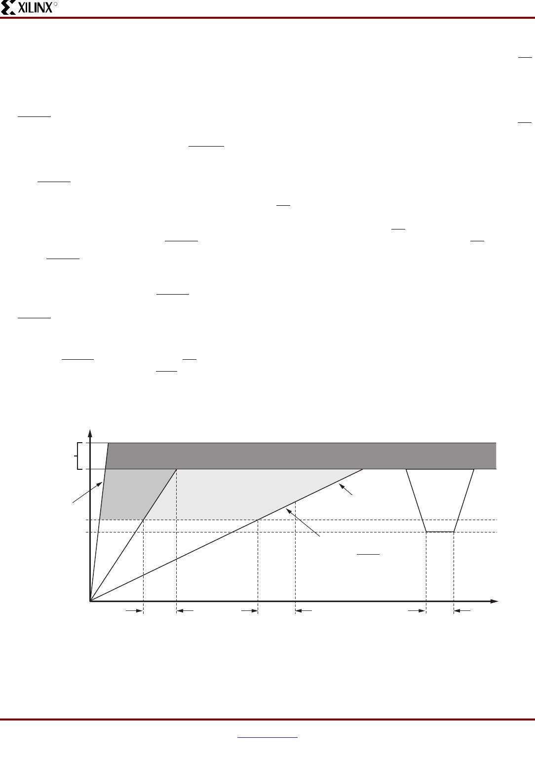
Reset and Power-On Reset Activation
At power up, the device requires the V
CCINT
power supply to
rise monotonically to the nominal operating voltage within
the specified V
CCINT
rise time. If the power supply cannot
meet this requirement, then the device might not perform
power-on reset properly. During the power-up sequence,
OE/RESET
is held Low by the PROM.
Once the required supplies have reached their respective
POR (Power On Reset) thresholds, the OE/RESET
release
is delayed (T
OER
minimum) to allow more margin for the
power supplies to stabilize before initiating configuration.
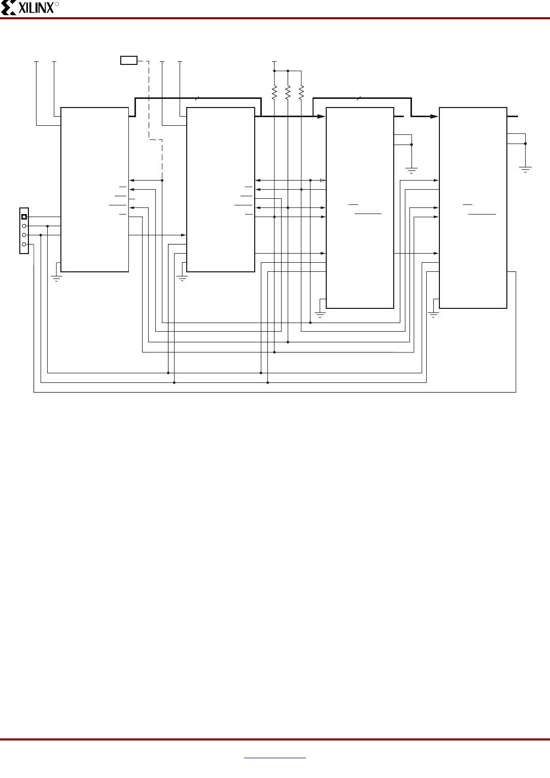
The OE/RESET
pin is connected to an external pull-up
resistor and also to the target FPGA's INIT_B pin. For
systems utilizing slow-rising power supplies, an additional
power monitoring circuit can be used to delay the target
configuration until the system power reaches minimum
operating voltages by holding the OE/RESET
pin Low.
When OE/RESET
is released, the FPGA’s INIT_B pin is
pulled High, allowing the FPGA's configuration sequence to
begin. If the power drops below the power-down threshold
(V
CCPD
), the PROM resets and OE/RESET is again held
Low until the after the POR threshold is reached.
OE/RESET
polarity is not programmable. These power-up
requirements are shown graphically in Figure 9.
For a fully powered Platform Flash PROM, a reset occurs
whenever OE/RESET
is asserted (Low) or CE is deasserted
(High). The address counter is reset, CEO
is driven High, and
the remaining outputs are placed in a high-Z state.
Standby Mode
The PROM enters a low-power standby mode whenever CE
is asserted High. The address is reset. The output remains
in a high-Z state regardless of the state of the OE input.
JTAG pins TMS, TDI and TDO can be in a high-Z state or
High. See Ta ble 7 .
When using the FPGA DONE signal to drive the PROM CE
pin High to reduce standby power after configuration, an
external pull-up resistor should be used. Typically a 330Ω
pull-up resistor is used, but refer to the appropriate FPGA
data sheet for the recommended DONE pin pull-up value. If
the DONE circuit is connected to an LED to indicate FPGA
configuration is complete, and also connected to the PROM
CE
pin to enable low-power standby mode, then an external
buffer should be used to drive the LED circuit to ensure valid
transitions on the PROMs CE
pin. If low-power standby
mode is not required for the PROM, then the CE
pin should
be connected to ground.
5V Tolerant I/Os
The I/Os on each re-programmable PROM are fully 5V tolerant
even through the core power supply is 3.3V. This allows 5V
CMOS signals to connect directly to the PROM inputs without
damage. In addition, the 3.3V V
CCINT
power supply can be
applied before or after 5V signals are applied to the I/Os. In
mixed 5V/3.3V/2.5V systems, the user pins, the core power
supply (V
CCINT
), and the output power supply (V
CCO
) can have
power applied in any order. This makes the PROM devices
immune to power supply sequencing issues.
X-Ref Target - Figure 9
Figure 9: V
CCINT
Power-Up Requirements
T
OER
V
CCINT
V
CCPOR
V
CCPD
200 µs ramp
50 ms ramp
T
OER
T
RST
TIME (ms)
A slow-ramping V
CCINT
supply may still
be below the minimum operating
voltage when OE/RESET is released.
In this case, the configuration
sequence must be delayed until both
V
CCINT
and V
CCO
have reached their
recommended operating conditions.
Recommended Operating Range
Delay or Restart
Configuration
ds026_20_032504
XC18V00 Series In-System-Programmable Configuration PROMs
DS026 (v5.2) January 11, 2008 www.xilinx.com
Product Specification 15
R
Customer Control Bits
The XC18V00 PROMs have various control bits accessible by the customer. These can be set after the array has been
programmed using “Skip User Array” in Xilinx iMPACT software. The iMPACT software can set these bits to enable the
optional JTAG read security, parallel configuration mode, or CF D4 pin function. See Ta ble 7 .
Absolute Maximum Ratings
(1,2)
Supply Voltage Requirements for Power-On Reset and Power-Down
Table 7: Truth Table for PROM Control Inputs
Control Inputs
Internal Address
Outputs
OE/RESET
CE DATA CEO I
CC
High Low If address < TC
(1)
: increment
If address > TC
(1)
: don’t change
Active
high-Z
High
Low
Active
reduced
Low Low Held reset High-Z High Active
High High Held reset High-Z High Standby
Low High Held reset High-Z High Standby
Notes:
1. TC = Terminal Count = highest address value. TC + 1 = address 0.
Symbol Description Value Units
V
CCINT/
V
CCO
Supply voltage relative to GND –0.5 to +4.0 V
V
IN
Input voltage with respect to GND –0.5 to +5.5 V
V
TS
Voltage applied to high-Z output –0.5 to +5.5 V
T
STG
Storage temperature (ambient) –65 to +150 ° C
T
J
Junction temperature +125 ° C
Notes:
1. Maximum DC undershoot below GND must be limited to either 0.5V or 10 mA, whichever is easier to achieve. During transitions, the device
pins can undershoot to –2.0V or overshoot to +7.0V, provided this over- or undershoot lasts less then 10 ns and with the forcing current being
limited to 200 mA.
2. Stresses beyond those listed under Absolute Maximum Ratings might cause permanent damage to the device. These are stress ratings
only, and functional operation of the device at these or any other conditions beyond those listed under Operating Conditions is not implied.
Exposure to Absolute Maximum Ratings conditions for extended periods of time might affect device reliability.
Symbol Description Min Max Units
T
VCC
V
CCINT
rise time from 0V to nominal voltage
(2)
0.2 50 ms
V
CCPOR
POR threshold for the V
CCINT
supply 1 V
T
OER
OE/RESET release delay following POR
(3)
01ms
T
RST
Time required to trigger a device reset when the V
CCINT
supply drops
below the maximum V
CCPD
threshold
10 ms
V
CCPD
Power-down threshold for V
CCINT
supply - 1 V
Notes:
1. V
CCINT
and V
CCO
supplies can be applied in any order.
2. At power up, the device requires the V
CCINT
power supply to rise monotonically to the nominal operating voltage within the specified T
VCC
rise
time. If the power supply cannot meet this requirement, then the device might not perform power-on-reset properly. See Figure 9, page 14.
3. If the V
CCINT
and V
CCO
supplies do not reach their respective recommended operating conditions before the OE/RESET pin is released,
then the configuration data from the PROM will not be available at the recommended threshold levels. The configuration sequence must be
delayed until both V
CCINT
and V
CCO
have reached their recommended operating conditions.
4. Typical POR is value is 2.0V.

XC18V01VQG44C

Mfr. #:
Manufacturer:
Xilinx
Description:
FPGA - Configuration Memory Re-programmable 1Mb PROM, Lead Free
Lifecycle:
New from this manufacturer.
Delivery:
DHL FedEx Ups TNT EMS
Payment:
T/T Paypal Visa MoneyGram Western Union