MIC2920A/29201/29202/29204 Micrel, Inc.
February 2005 5 M9999-021505
Notes:
General: Devices are ESD protected; however, handling precautions are recommended.
Note 1: Absolute maximum ratings indicate limits beyond which damage to the component may occur. Electrical specifications do not apply when
operating the device outside of its rated operating conditions. The maximum allowable power dissipation is a function of the maximum
junction temperature, T
J (MAX)
, the junction-to-ambient thermal resistance, θ
JA
, and the ambient temperature, T
A
. The maximum allowable
power dissipation at any ambient temperature is calculated using: P
(MAX)
= (T
J(MAX)
– T
A
)
/ θ
JA.
Exceeding the maximum allowable power
dissipation will result in excessive die temperature, and the regulator will go into thermal shutdown. The junction to ambient thermal
resistance of the MIC29204BM is 160°C/W mounted on a PC board.
Note 2: Output voltage temperature coefficient is defined as the worst case voltage change divided by the total temperature range.
Note 3: Regulation is measured at constant junction temperature using low duty cycle pulse testing. Changes in output voltage due to heating effects
are covered by the thermal regulation specification.
Note 4: Dropout Voltage is defined as the input to output differential at which the output voltage drops 100mV below its nominal value measured at
1V differential. At low values of programmed output voltage, the minimum input supply voltage of 4.3V over temperature must be taken into
account. The MIC2920A operates down to 2V of input at reduced output current at 25°C.
Note 5: Ground pin current is the regulator quiescent current. The total current drawn from the supply is the sum of the load current plus the ground
pin current.
Note 6: The MIC2920A features fold-back current limiting. The short circuit (V
OUT
= 0V) current limit is less than the maximum current with normal
output voltage.
Note 7: Thermal regulation is defined as the change in output voltage at a time T after a change in power dissipation is applied, excluding load or
line regulation effects. Specifications are for a 200mA load pulse at V
IN
= 20V (a 4W pulse) for T = 10ms.
Note 8: V
REF
≤ V
OUT
≤ (V
IN
– 1 V), 4.3V ≤ V
IN
≤ 26V, 1 mA < I
L
≤400 mA, T
J
≤ T
J MAX.
Note 9: Comparator thresholds are expressed in terms of a voltage differential at the Adjust terminal below the nominal reference voltage measured
at 6V input. To express these thresholds in terms of output voltage change, multiply by the error amplifier gain = V
OUT
/V
REF
= (R1 + R2)/R2.
For example, at a programmed output voltage of 5V, the Error output is guaranteed to go low when the output drops by 95 mV x 5V/1.235 V
= 384 mV. Thresholds remain constant as a percent of V
OUT as VOUT is varied, with the dropout warning occurring at typically 5% below
nominal, 7.7% guaranteed.
Note 10: V
SHUTDOWN
≥ 2V, V
IN
≤ 26V,V
OUT
= 0, with Adjust pin tied to 5V Tap or to the R1, R2 junction (see Figure 3) with R1 ≥ 150kΩ.
Note 11: When used in dual supply systems where the regulator load is returned to a negative supply, the output voltage must be diode clamped to
ground.
Note 12: Maximum positive supply voltage of 60V must be of limited duration (< 100ms) and duty cycle ( ≤ 1%). The maximum continuous supply
voltage is 26V.
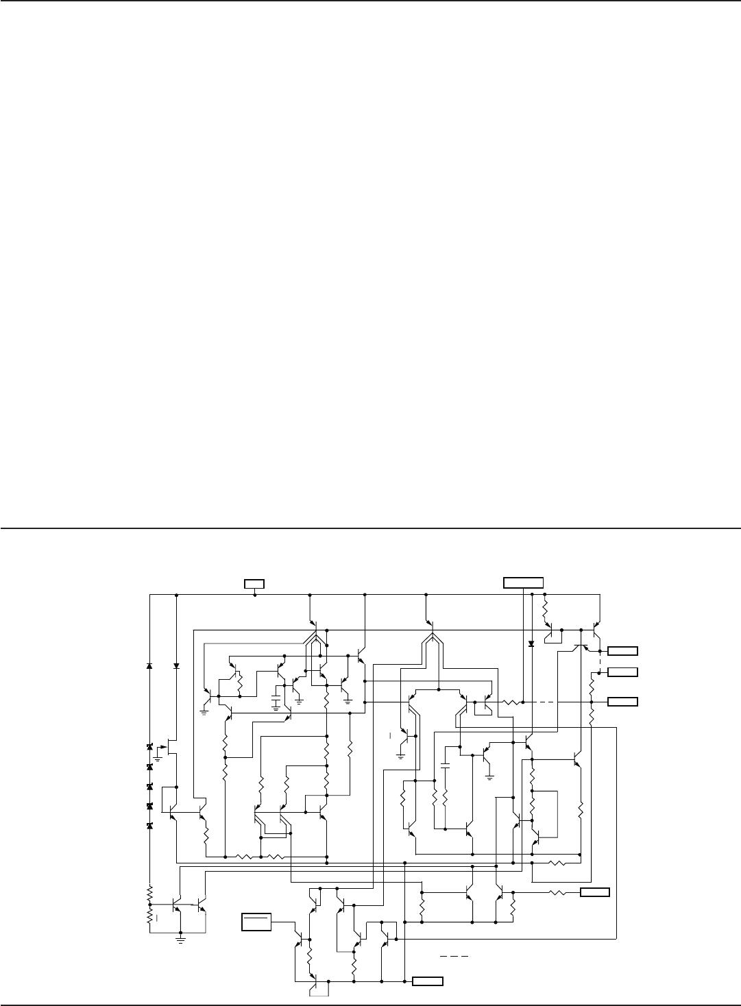
AD JU ST
S E NS E
Q15A
OUT
Q24
Q26
R27
V TAP
R28
R18
20k
Ω
Q25
Q23
Q22
R15
100
kΩ
R16
30
kΩ
Q29
Q28
R17
10
Ω
R21 8 Ω
R17
12
kΩ
Q31
Q30
R23 60 kΩ
SHDN
R24
50
kΩ
R22
150
kΩ
Q21
Q19
C2
40 pF
R14
350
kΩ
Q14
R13
100
kΩ
Q18
R12
110
kΩ
Q20
Q9
Q15 B
Q8
Q7
R11
20.6
kΩ
Q5
R8
31.4 kΩ
R10
150
kΩ
R9
27.8
kΩ
Q11
Q12
Q13
R6
140
kΩ
R5
180
kΩ
R4
13
kΩ
R3
50
kΩ
Q2
C1
20
pF
Q4
Q3
R11
18
kΩ
Q6
Q1
10
R1
20
kΩ
R2
50
kΩ
Q41
R30
30
kΩ
Q40
Q34
GND
Q36
Q37
R25
2.8
kΩ
Q38
E RR O R
R26
60
kΩ
Q39
Q42
Q16
Q17
50 kΩ
10
kΩ
IN
DENO T E S C O NN E C T I ON ON
MIC2920A-xx AND MIC29201-xx
VE R S I ONS ON L Y
Schematic Diagram