MIC2920A/29201/29202/29204 Micrel, Inc.
M9999-021505 8 February 2005
or some other supply voltage. In determining a value for this
resistor, note that while the output is rated to sink 250µA, this
sink current adds to battery drain in a low battery condition.
Suggested values range from 100k to 1MΩ. The resistor is
not required if this output is unused.
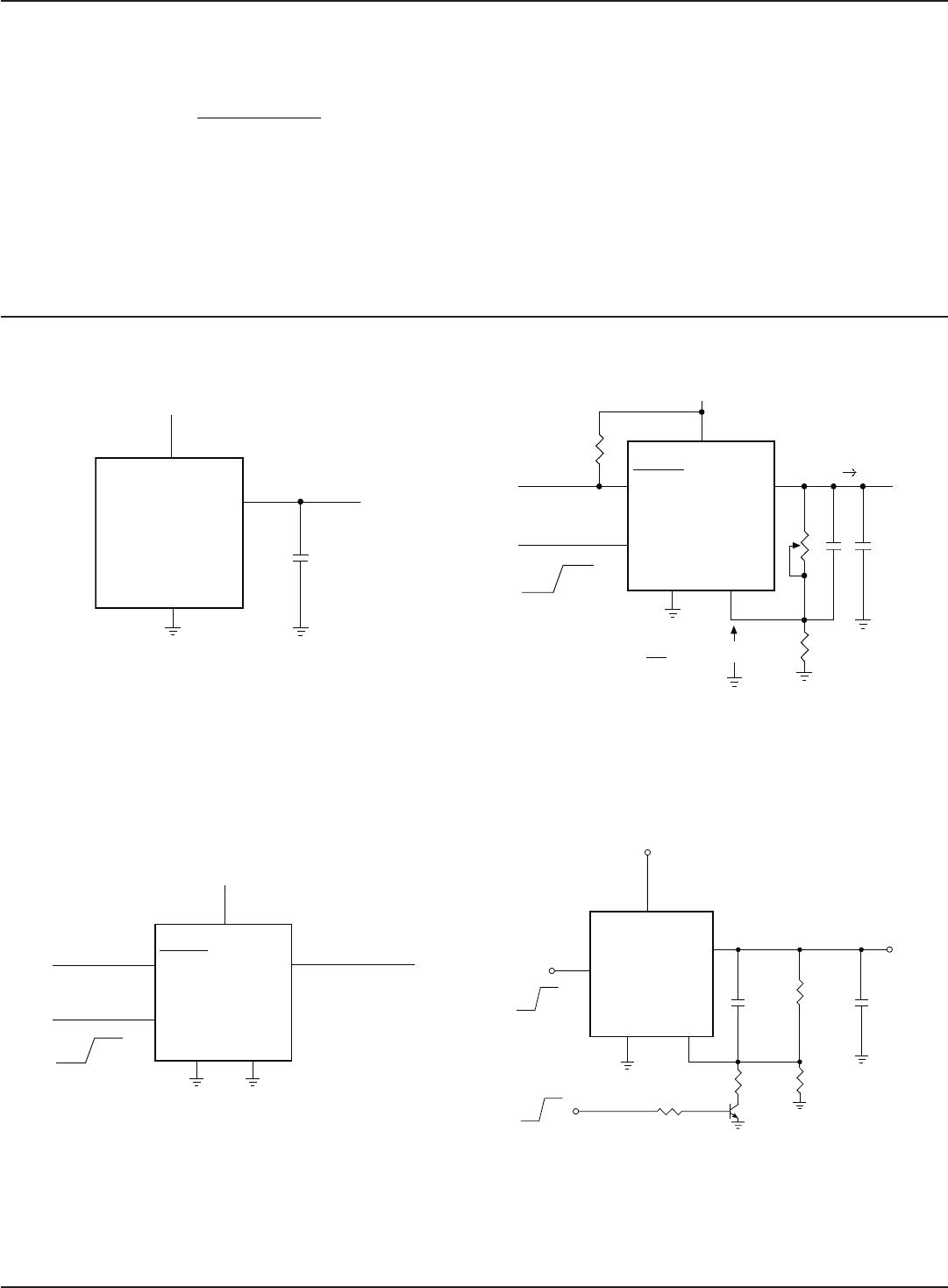
Programming the Output Voltage
(MIC29202/29204)
The MIC29202/29204 may be programmed for any output
voltage between its 1.235V reference and its 26V maxi-
mum rating, using an external pair of resistors, as shown in
Figure 3.
The complete equation for the output voltage is
V
OUT
= V
REF
× { 1 + R
1
/R
2
} – |I
FB
| R
1
where V
REF
is the nominal 1.235 reference voltage and I
FB
is
the Adjust pin bias current, nominally 20nA. The minimum rec-
ommended load current of 1µA forces an upper limit of 1.2MΩ
on the value of R
2
, if the regulator must work with no load (a
condition often found in CMOS in standby), I
FB
will produce
a –2% typical error in V
OUT
which may be eliminated at room
temperature by trimming R
1
. For better accuracy, choosing R
2
= 100k reduces this error to 0.17% while increasing the resistor
program current to 12µA. Since the MIC29202/29204 typically
draws 110µA at no load with SHUTDOWN open-circuited, this
is a negligible addition. The MIC29204 may be pin-strapped
for 5V using the internal voltage divider by tying Pin 1 (output)
to Pin 2 (sense) and Pin 7 (Adjust) to Pin 6 (V Tap).
Configuring the MIC29201-3.3BM
For the MIC29201-3.3BM, the output (Pin 1) and sense pin
(pin 2), must be connected to ensure proper operation. They
are not connected internally.
Reducing Output Noise
In reference applications it may be advantageous to reduce
the AC noise present at the output. One method is to reduce
the regulator bandwidth by increasing the size of the output
capacitor. This is relatively inefficient, as increasing the capaci-
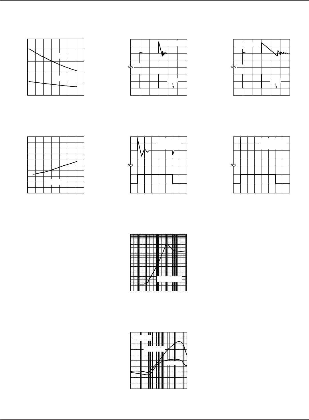
Figure 1. ERROR Output Timing
* SEE APPLICATIONS INFORMATION
Applications Information
External Capacitors
A 10µF (or greater) capacitor is required between the MIC2920A
output and ground to prevent oscillations due to instability. Most
types of tantalum or aluminum electrolytics will be adequate;
film types will work, but are costly and therefore not recom-
mended. Many aluminum electrolytics have electrolytes that
freeze at about –30°C, so solid tantalums are recommended
for operation below –25°C. The important parameters of the
capacitor are an effective series resistance of about 5Ω or
less and a resonant frequency above 500kHz. The value of
this capacitor may be increased without limit.
At lower values of output current, less output capacitance is
required for output stability. The capacitor can be reduced
to 2.2µF for current below 10mA or 1µF for currents below
1mA. Adjusting the MIC29202/29204 to voltages below 5V
runs the error amplifier at lower gains so that more output ca-
pacitance is needed. For the worst-case situation of a 500mA
load at 1.23V output (Output shorted to Adjust) a 47µF (or
greater) capacitor should be used.
The MIC2920A/29201 will remain in regulation with a mini
-
mum load of 1mA. When setting the output voltage of the
MIC29202/29204 versions with external resistors, the current
through these resistors may be included as a portion of the
minimum load.
A 0.1µF capacitor should be placed from the MIC2920A input
to ground if there is more than 10 inches of wire between
the input and the AC filter capacitor or if a battery is used as
the input.
Error Detection Comparator Output
(MIC29201/MIC29204)
A logic low output will be produced by the comparator when-
ever the MIC29201/29204 output falls out of regulation by
more than approximately 5%. This figure is the comparator’s
built-in offset of about 75mV divided by the 1.235V reference
voltage. (Refer to the block diagram on Page 1). This trip level
remains “5% below normal” regardless of the programmed
output voltage of the MIC29201/29204. For example, the
error flag trip level is typically 4.75V for a 5V output or 11.4V
for a 12V output. The out of regulation condition may be due
either to low input voltage, extremely high input voltage, cur-
rent limiting, or thermal limiting.
Figure 1 is a timing diagram depicting the ERROR signal and
the regulated output voltage as the MIC29201/29204 input is
ramped up and down. The ERROR signal becomes valid (low)
at about 1.3V input. It goes high at about 5V input (the input
voltage at which V
OUT
= 4.75). Since the MIC29201/29204’s
dropout voltage is load-dependent (see curve in Typical Per-
formance Characteristics), the input voltage trip point (about
5V) will vary with the load current. The output voltage trip point
(approximately 4.75V) does not vary with load.
The error comparator has an NPN open-collector output which
requires an external pull-up resistor. Depending on system
requirements, this resistor may be returned to the 5V output
4.75V
E R R O R
OUTPU T
VOLTAGE
IN PUT
5V
1.3V
VOLTAGE
NOT *
VALID
NOT *
VALID