NJG1512V-TE1

NJG1512V
- 1 -
SPDT SWITCH GaAs MMIC
nGENERAL DESCRIPTION nPACKAGE OUTLINE
NJG1512V is a GaAs SPDT switch IC featuring high
isolation and low insertion loss.
This switch allows low operating voltage from 2.5V at
the wide frequency range from 1MHz to 3GHz.
NJG1512V is suitable to switch the synthesizer
signals between transmit and receiving circuit.
A very small SSOP package is adopted.
nFEATURES
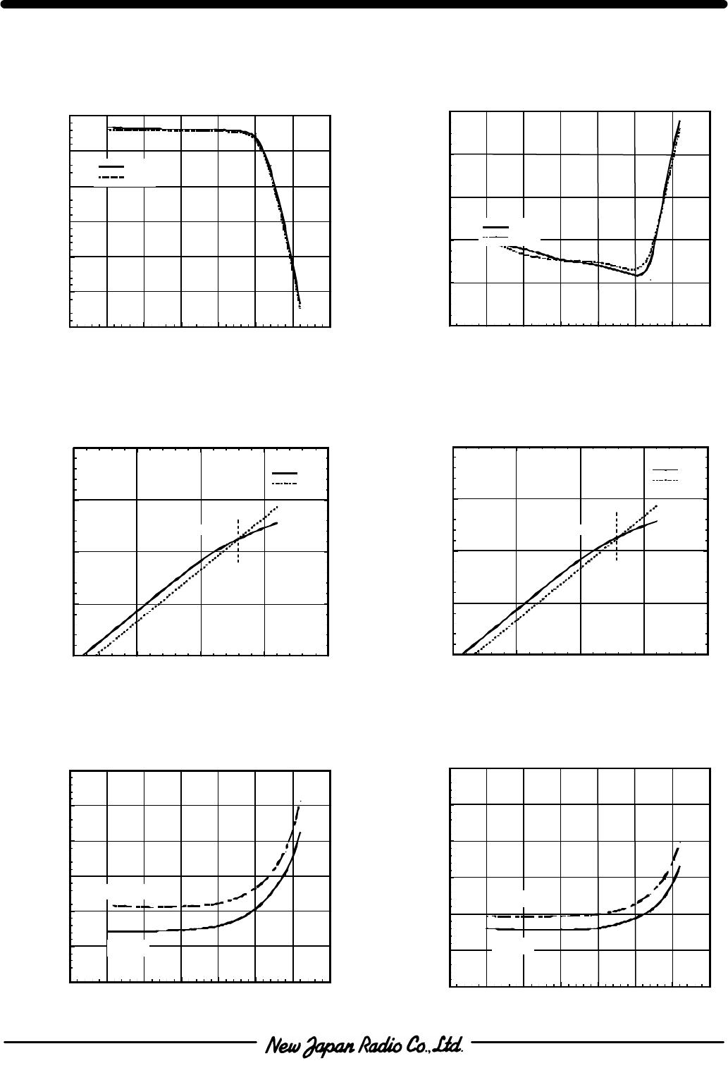
lSingle, low voltage control +2.5~+5.5V
lHigh isolation 46dB typ. @f=0.05~2GHz, P
in
=0dBm
lLow insertion loss 0.8dB typ. @f=2GHz, P
in
=0dBm
lLow current consumption 2uA typ. @f=0.05~2.5GHz, P
in
=10dBm
lPackage SSOP14 (Mount Size: 6.4x5.0x1.25mm)
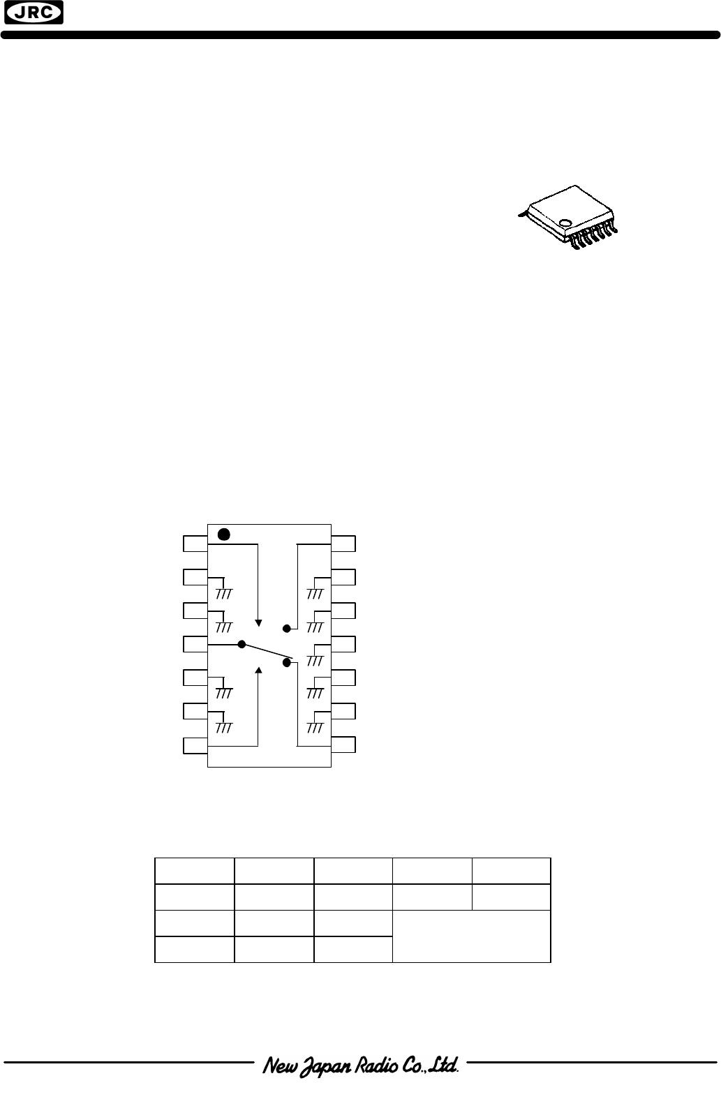
nPIN CONFIGURATION
nTRUTH TABLE
V
CTR1
H L L H
V
CTR2
L H L H
PC-P1 OFF ON
PC-P2 ON OFF
*1
“H”=V
CTR (H),
“L”=V
CTR (L)
NJG1512V
*1) Combinations of V
CTR1
/V
CTR2
=L/L, H/H are not available.
Pin Connection
1. V
CTR2
2. GND
3. GND
4. PC
5. GND
6. GND
7. V
CTR1
8. P1
9. GND
10. GND
11. GND
12. GND
13. GND
14. P2
V Type
(Top View)
1
2
3
4
5
6
7
14
13
12
11
10
9
8
NJG1512V
- 2 -
nABSOLUTE MAXIMUM RATINGS
(T
a
=25°C, Z
s
=Z
l
=50)
PARAMETER SYMBOL
RATINGS UNITS
Input Power
P
in
27 dBm
Control Voltage
V
CTR
6.0 V
Power Dissipation
P
D
600 mW
Operating Temp.
T
opr
-20~+85 °C
Storage Temp.
T
stg
-40~+150 °C
nELECTRICAL CHARACTERISTICS 1
(TEST CIRCUIT 1: V
CTR (L)
=0V, V
CTR (H)
=2.7V, Z
s
=Z
o
=50, T
a
=25°C)
PARAMETER SYMBOL
CONDITIONS MIN TYP MAX UNITS
Control voltage (L) V
CTR (L)
f=0.05~2.5GHz, P
in
=10dBm -0.2 0 0.2 V
Control voltage (H) V
CTR (H)
f=0.05~2.5GHz, P
in
=10dBm 2.5 2.7 5.5 V
Control current I
CTR
f=0.05~2.5GHz, P
in
=10dBm - 2.0 4.0 uA
Isolation ISL1 f=0.05~2.0GHz, P
in
=0dBm 43 46 - dB
Insertion loss 1 LOSS1 f=1.0GHz, P
in
=0dBm - 0.6 1.0 dB
Insertion loss 2 LOSS2 f=2.0GHz, P
in
=0dBm - 0.8 1.2 dB
Pin at 1dB
compression point
P
-1dB
f=2.0GHz 19.0 22.0 - dBm
VSWR VSWR f=0.05~2.5GHz, ON STATE - 1.2 1.8
Switching time T
SW
f=0.05~2.5GHz - 8 - ns
nELECTRICAL CHARACTERISTICS 2
(TEST CIRCUIT 2: V
CTR (L)
=0V, V
CTR (H)
=2.7V, Z
s
=Z
o
=50, T
a
=25°C)
PARAMETER SYMBOL
CONDITIONS MIN TYP MAX UNITS
Isolation 2 ISL2 f=1~100MHz, P
in
=0dBm - 55 - dB
Insertion loss 3 LOSS3 f=1~100MHz, P
in
=0dBm - 0.5 - dB
NJG1512V
- 3 -
10
15
20
25
30
10 15 20 25 30
Pout
P-1
Output Power (dBm)
Input Power (dBm)
P-1(in) = 23.15 dBm
(PC-P2) P
in
vs. P
out
(V
CTR
=0V/2.7V, f
in
=2.0GHz)
10
15
20
25
30
10 15 20 25 30
Pout
P-1
Output Power (dBm)
Input Power (dBm)
P-1(in) = 23.16 dBm
(PC-P1) P
in
vs. P
out
(V
CTR
=0V/2.7V, f
in
=2.0GHz)
nTYPICAL CHARACTERISTICS
-3.5
-3
-2.5
-2
-1.5
-1
-0.5
-5
0
5
10
15
20
25
30
PC-P1
PC-P2
Insertion Loss:LOSS (dB)
Input Power (dBm)
P
in
vs. Insertion Loss
(V
CTR
=0V/2.7V,f
in
=2GHz)
-50
-48
-46
-44
-42
-40
-5
0
5
10
15
20
25
30
PC-P1
PC-P2
Isolation:ISL (dB)
Input Power (dBm)
P
in
vs. Isolation
(V
CTR
=0V/2.7V,f
in
=2GHz)
0
1
2
3
4
5
6
-5
0
5
10
15
20
25
30
Control Current:I
CTR
(uA)
Input Power (dBm)
V
CTR
=2.7V
V
CTR
=2.5V
(PC-P1) P
in
vs. I
CTR
(f
in
=2GHz)
0
1
2
3
4
5
6
-5
0
5
10
15
20
25
30
Control Current:I
CTR
(uA)
Input Power (dBm)
V
CTR
=2.7V
V
CTR
=2.5V
(PC-P2) P
in
vs. I
CTR
(f
in
=2GHz)

NJG1512V-TE1

Mfr. #:
Manufacturer:
NJR (New Japan Radio)
Description:
RF Switch ICs SPDT Switch
Lifecycle:
New from this manufacturer.
Delivery:
DHL FedEx Ups TNT EMS
Payment:
T/T Paypal Visa MoneyGram Western Union

Products related to this Datasheet