ICS9EPRS525
IDT
TM
56-pin CK505 for Embedded Intel Systems 1614B—01/21/10
56-pin CK505 for Embedded Intel Systems
1
DATASHEET
Pin Configuration
Recommended Application:
56-pin CK505 compatible clock, w/fully integrated Vreg and series
resistors on differential outputs for embedded applications
Output Features:
2 - CPU differential low power push-pull pairs
7 - SRC differential push-pull pairs
1 - CPU/SRC selectable differential low power push-pull pair
1 - SRC/DOT selectable differential low power push-pull pair
1 - SRC/SE selectable differential push-pull pair/Single-ended
outputs
5 - PCI, 33MHz
1 - USB, 48MHz
1 - REF, 14.318MHz
Key Specifications:
CPU outputs cycle-cycle jitter < 85ps
SRC output cycle-cycle jitter < 125ps
PCI outputs cycle-cycle jitter < 250ps
+/- 100ppm frequency accuracy on all outputs
SRC outputs meet PCIe Gen2 when sourced from PLL3
Features/Benefits:
Supports spread spectrum modulation, 0 to -0.5% down
spread
Supports CPU clks up to 400MHz
Uses external 14.318MHz crystal, external crystal load
caps are required for frequency tuning
Table 1: CPU Frequency Select Table
FS
L
C
2
B0b7
FS
L
B
1
B0b6
FS
L
A
1
B0b5
CPU
MHz
SRC
MHz
PCI
MHz
REF
MHz
USB
MHz
DOT
MHz
0 0 0 266.66
0 0 1 133.33
0 1 0 200.00
0 1 1 166.66
1 0 0 333.33
1 0 1 100.00
1 1 0 400.00
111
1. FS
L
A and FS
L
B are low-threshold inputs.Please see V
IL_FS
and V
IH_FS
specifications in
the Input/Supply/Common Output Parameters Table for correct values.
Also refer to the Test Clarification Table.
2. FS
L
C is a three-level input. Please see the V
IL_FS
and V
IH_FS
specifications in the Input/Supply/Common Output Parameters Table for correct values.
Reserved
100.00 33.33 14.318 48.00 96.00
PCI0/CR#_A 1 56 SCLK
VDDPCI 2 55 SDATA
PCI1/CR#_B 3 54 REF0/FSLC/TEST_SEL
PCI2/TME 4 53 VDDREF
PCI3/CFG0 5 52 X1
PCI4/SRC5_EN 6 51 X2
PCI_F5/ITP_EN 7 50 GNDREF
GNDPCI 8 49 FSLB/TEST_MODE
VDD48 9 48 CK_PWRGD/PD#
USB_48MHz/FSLA 10 47 VDDCPU
GND4811 46CPUT0_LRS
VDD96IO 12 45 CPUC0_LRS
DOTT_96_LRS/SRCT0_LRS 13 44 GNDCPU
DOTC_96_LRS/SRCC0_LRS 14 43 CPUT1_F_LRS
GND 15 42 CPUC1_F_LRS
VDD 16 41 VDDCPUIO
SRCT1_LRS/SE1 17 40 NC
SRCC1_LRS/SE2 18 39 CPUT2_ITP_LRS/SRCT8_LRS
GND 19 38 CPUC2_ITP_LRS/SRCC8_LRS
VDDPLL3IO 20 37 VDDSRCIO
SRCT2_LRS/SATAT_LRS 21 36 SRCT7_LRS/CR#_F
SRCC2_LRS/SATAC_LRS 22 35 SRCC7_LRS/CR#_E
GNDSRC 23 34 GNDSRC
SRCT3_LRS/CR#_C 24 33 SRCT6_LRS
SRCC3_LRS/CR#_D 25 32 SRCC6_LRS
VDDSRCIO 26 31 VDDSRC
SRCT4_LRS 27 30 PCI_STOP#/SRCT5_LRS
SRCC4_LRS 28 29 CPU_STOP#/SRCC5_LRS
56-TSSOP
9EPRS525
IDT
TM
56-pin CK505 for Embedded Intel Systems 1614B—01/21/10
ICS9EPRS525
2
56-pin CK505 for Embedded Systems
Pin Description
PIN # PIN NAME TYPE DESCRIPTION
1 PCI0/CR#_A I/O
3.3V PCI clock output or Clock Request control A for either SRC0 or SRC2 pair
The power-up default is PCI0 output, but this pin may also be used as a Clock Request control of SRC pair 0 or SRC pair 2 via SMBus. Before
configuring this pin as a Clock Request Pin, the PCI output must first be disabled in byte 2, bit 0 of SMBus address space . After the PCI output is
disabled (high-Z), the pin can then be set to serve as a Clock Request pin for either SRC pair 2 or pair 0 using the CRA#_EN bit located in byte 5 of
SMBUs address space.
Byte 5, bit 7
0 = PCI0 enabled (default)
1= CRA# enabled. Byte 5, bit 6 controls whether CRA# controls SRC0 or SRC2 pair
Byte 5, bit 6
0 = CRA# controls SRC0 pair (default),
1= CRA# controls SRC2 pair
2 VDDPCI PWR Power supply for PCI clocks, nominal 3.3V
3 PCI1/CR#_B I/O
3.3V PCI clock output/Clock Request control B for either SRC1 or SRC4 pair
The power-up default is PCI1 output, but this pin may also be used as a Clock Request control of SRC pair 1 or SRC pair 4 via SMBus. Before
configuring this pin as a Clock Request Pin, the PCI output must first be disabled in byte 2, bit 1 of SMBus address space . After the PCI output is
disabled (high-Z), the pin can then be set to serve as a Clock Request pin for either SRC pair 1 or pair 4 using the CRB#_EN bit located in byte 5 of
SMBUs address space.
Byte 5, bit 5
0 = PCI1 enabled (default)
1= CRB# enabled. Byte 5, bit 6 controls whether CRB# controls SRC1 or SRC4 pair
Byte 5, bit 4
0 = CRB# controls SRC1 pair (default)
1= CRB# controls SRC4 pair
4PCI2/TME I/O
3.3V PCI clock output / Trusted Mode Enable(TME) Latched Input. This pin is sampled on power-up as follows
0=Overclocking of CPU and SRC allowed
1=Overclocking of CPU and SRC NOT allowed
After being sampled on power-up, this pin becomes a 3.3V PCI Output
5 PCI3/CFG0 I/O 3.3V PCI clock output/Configuration Strap. See PCI3 Configuration Table for more information
6 PCI4/SRC5_EN I/O
3.3V PCI clock output / SRC5 pair or PCI_STOP#/CPU_STOP# enable strap. On powerup, the logic value on this pin determines if the SRC5 pair is
enabled or if CPU_STOP#/PCI_STOP# is enabled (pins 29 and 30). The latched value controls the pin function on pins 29 and 30 as follows
0 = PCI_STOP#/CPU_STOP#
1 = SRC5/SRC5#
7 PCI_F5/ITP_EN I/O
Free running PCI clock output and ITP/SRC8 enable strap. This output is not affected by the state of the PCI_STOP# pin. On powerup, the state of
this pin determines whether pins 38 and 39 are an ITP or SRC pair.
0 =SRC8/SRC8#
1 = ITP/ITP#
8 GNDPCI PWR Ground pin for the PCI outputs
9 VDD48 PWR Power pin for the 48MHz output and PLL.3.3V
10 USB_48MHz/FSLA I/O
3.3V tolerant input for CPU frequency selection. Refer to input electrical characteristics for Vil_FS and Vih_FS values. / Fixed 48MHz USB clock
out
p
ut. 3.3V.
11 GND48 PWR Ground pin for the 48MHz outputs
12 VDD96IO PWR Power supply for DOT96 outputs, 1.05V to 3.3V.
13 DOTT_96_LRS/SRCT0_LRS OUT
True clock of low power differential SRC or DOT96 with integrated 33 ohm Rs. The power-up default function is SRC0. After powerup, this pin function
may be changed to DOT96 via SMBus Byte 1, bit 7 as follows:
0= SRC0
1=DOT96
14 DOTC_96_LRS/SRCC0_LRS OUT
Complement clock of low power differential SRC or DOT96 with integrated 33 ohm Rs. The power-up default function is SRC0#. After powerup, this
pin function may be changed to DOT96# via SMBus Byte 1, bit 7 as follows
0= SRC0#
1=DOT96#
15 GND PWR Ground pin.
16 VDD PWR Power supply, nominal 3.3V
17 SRCT1_LRS/SE1 OUT
True clock of low power differential SRC1 clock pair with integrated 33 ohm Rs. / 3.3V single-ended output. The powerup default is 100 MHz SRC, -
0.5% downs
p
read. The
p
in function ma
y
be chan
g
ed via SMBus B1b
[
4:1
]
18 SRCC1_LRS/SE2 OUT
Complement clock of low powerl differential SRC1 clock pair with integrated 33 ohm Rs / 3.3V single-ended output. The powerup default is 100 MHz
SRC
,
-0.5% downs
p
read. The
p
in function ma
y
be chan
g
ed via SMBus B1b
[
4:1
]
19 GND PWR Ground pin.
20 VDDPLL3IO PWR Power supply for PLL3 outputs. 1.05V to 3.3V.
21 SRCT2_LRS/SATAT_LRS OUT True clock of low power differentiall SRC/SATA clock pair with integrated Rs.
22 SRCC2_LRS/SATAC_LRS OUT Complement clock of low power differential push-pull SRC/SATA clock pair with integrated 33 ohm Rs.
23 GNDSRC PWR Ground pin for the SRC outputs
24 SRCT3_LRS/CR#_C I/O
True clock of low power differential SRC clock pair with integrated 33 ohm Rs./ Clock Request control C for either SRC0 or SRC2 pair. The power-up
default is SRCCLK3 output, but this pin may also be used as a Clock Request control of SRC pair 0 or SRC pair 2 via SMBus. Before configuring this
pin as a Clock Request Pin, the SRC output must first be disabled in byte 4, bit 7 of SMBus address space . After the SRC output is disabled, the pin
can then be set to serve as a Clock Request pin for either SRC pair 2 or pair 0 using the CRC#_EN bit located in byte 5 of SMBUs address space.
Byte 5, bit 3
0 = SRCCLK3 enabled (default)
1= CRC# enabled. Byte 5, bit 2 controls whether CRC# controls SRC0 or SRC2 pair
Byte 5, bit 2
0 = CRC# controls SRC0 pair (default),
1= CRC# controls SRC2 pair
IDT
TM
56-pin CK505 for Embedded Intel Systems 1614B—01/21/10
ICS9EPRS525
3
56-pin CK505 for Embedded Systems
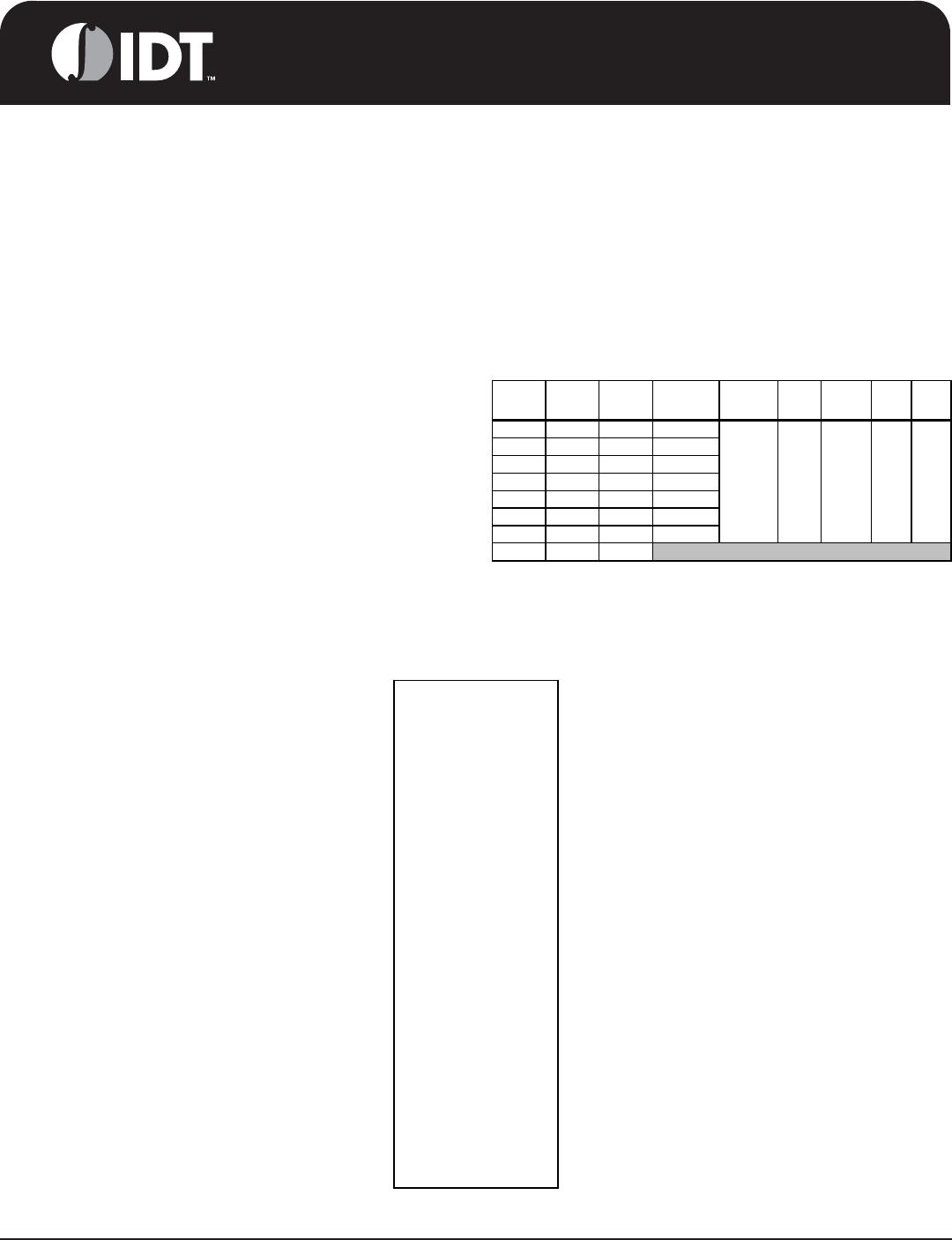
Pin Description (continued)
PIN # PIN NAME TYPE DESCRIPTION
25 SRCC3_LRS/CR#_D I/O
Complementary clock of low power differential SRC clock pair with integrated 33 ohm Rs/ Clock Request control D for either SRC1 or SRC4 pair.
The power-up default is SRCCLK3 output, but this pin may also be used as a Clock Request control of SRC pair 1 or SRC pair 4 via SMBus. Before
configuring this pin as a Clock Request Pin, the SRC output must first be disabled in byte 4, bit 7 of SMBus address space . After the SRC output is
disabled, the pin can then be set to serve as a Clock Request pin for either SRC pair 1 or pair 4 using the CRD#_EN bit located in byte 5 of SMBUs
address space.
Byte 5, bit 1
0 = SRC3 enabled (default)
1= CRD# enabled. Byte 5, bit 0 controls whether CRD# controls SRC1 or SRC4 pair
Byte 5, bit 0
0 = CRD# controls SRC1 pair (default),
1= CRD# controls SRC4
p
air
26 VDDSRCIO PWR Power supply for SRC outputs. 1.05V to 3.3V.
27 SRCT4_LRS OUT True clock of low power differential SRC clock pair with integrated 33 ohm Rs.
28 SRCC4_LRS OUT Complement clock of low power differential SRC clock pair with 33 ohm integrated Rs.
29 CPU_STOP#/SRCC5_LRS I/O
Stops all CPUCLK, except those set to be free running clocks /
Com
p
lement clock of low
p
ower differential SRC
p
air with 33 ohm inte
g
rated Rs.
30 PCI_STOP#/SRCT5_LRS I/O
Stops all PCICLKs at logic 0 level, when low. Free running PCICLKs are not effected by this input. / True clock of low power differential SRC pair
with inte
g
rated 33 ohm Rs.
31 VDDSRC PWR Supply for SRC PLL, 3.3V nominal
32 SRCC6_LRS OUT Complement clock of low power differential SRC clock pair with 33 ohm integrated Rs.
33 SRCT6_LRS OUT True clock of low power differential SRC clock pair with integrated 33 ohm Rs.
34 GNDSRC PWR Ground pin for the SRC outputs
35 SRCC7_LRS/CR#_E I/O
Complement clock of differential push-pull SRC clock pair with 33 ohm integrated Rs. / Clock Request control E for SRC6 pair. The power-up default
is SRC7#, but this pin may also be used as a Clock Request control of SRC6 via SMBus. Before configuring this pin as a Clock Request Pin, the
SRC7 output pair must first be disabled in byte 3, bit 3 of SMBus configuration space . After the SRC output is disabled (high-Z), the pin can then be
set to serve as a Clock Request for SRC6 pair using byte 6, bit 7 of SMBus configuration space
Byte 6, bit 7
0 = SRC7# enabled (default)
1= CRE# enabled.
36 SRCT7_LRS/CR#_F I/O
True clock of differential push-pull SRC clock pair/ Clock Request control 8 for SRC8 pair
The power-up default is SRC7, but this pin may also be used as a Clock Request control of SRC8 via SMBus. Before configuring this pin as a Clock
Re
q
uest Pin
,
the SR
37 VDDSRCIO PWR Power supply for SRC outputs. 1.05V to 3.3V.
38 CPUC2_ITP_LRS/SRCC8_LRS OUT
Complement clock of low power differential CPU2/Complement clock of differential SRC pair. 33 ohm Rs is integrated. The function of this pin is
determined by the latched input value on pin 7, PCIF5/ITP_EN on powerup. The function is as follows:
Pin 7 latched input Value
0 = SRC8#
1 = ITP#
39 CPUT2_ITP_LRS/SRCT8_LRS OUT
True clock of low power differential CPU2/True clock of differential SRC pair. 33 ohm Rs is integrated. The function of this pin is determined by the
latched input value on pin 7, PCIF5/ITP_EN on powerup. The function is as follows:
Pin 7 latched input Value
0 = SRC8
1 = ITP
40 NC
N/A No Connect
41 VDDCPUIO PWR Power supply for CPU outputs, 1.05V to 3.3V.
42 CPUC1_F_LRS OUT Complementary clock of low power differential push-pull CPU output with integrated 33 ohm Rs. This CPU clock is free running during iAMT.
43 CPUT1_F_LRS OUT True clock of differential push-pull CPU clock pair with integrated 33 ohm Rs. This clock is free running during iAMT.
44 GNDCPU PWR Ground pin for the CPU outputs
45 CPUC0_LRS OUT Complement clock of low power differential CPU clock pair with integrated 33 ohm Rs.
46 CPUT0_LRS OUT True clock of low power differential CPU clock pair with integrated 33 ohm Rs.
47 VDDCPU PWR Supply for CPU PLL, 3.3V nominal
48 CK_PWRGD/PD# IN Notifies CK505 to sample latched inputs, or iAMT entry/exit, or PWRDWN# mode
49 FSLB/TEST_MODE IN
3.3V tolerant input for CPU frequency selection. Refer to input electrical characteristics for Vil_FS and Vih_FS values. TEST_MODE is a real time
in
ut to select between Hi-Z and REF/N divider mode while in test mode. Refer to Test Clarification Table.
50 GNDREF PWR Ground pin for the REF outputs.
51 X2 OUT Crystal output, Nominally 14.318MHz
52 X1 IN Crystal input, Nominally 14.318MHz.
53 VDDREF PWR Ref, XTAL power supply, nominal 3.3V
54 REF0/FSLC/TEST_SEL I/O
14.318 MHz reference clock./ 3.3V tolerant input for CPU frequency selection. Refer to input electrical characteristics for Vil_FS and Vih_FS values.
/TEST_Sel: 3-level latched in
p
ut to enable test mode. Refer to Test Clarification Table
55 SDATA I/O Data pin for SMBus circuitry, 5V tolerant.
56 SCLK IN Clock pin of SMBus circuitry, 5V tolerant.

9EPRS525AGILFT

Mfr. #:
Manufacturer:
IDT
Description:
Clock Synthesizer / Jitter Cleaner EMBEDDED 56P CK505 COMPATIBLE
Lifecycle:
New from this manufacturer.
Delivery:
DHL FedEx Ups TNT EMS
Payment:
T/T Paypal Visa MoneyGram Western Union

Products related to this Datasheet