TC74LCX14FK(EL,K)

TC74LCX14F/FT/FK
2014-03-01
1
TOSHIBA CMOS Digital Integrated Circuit Silicon Monolithic
TC74LCX14F, TC74LCX14FT, TC74LCX14FK
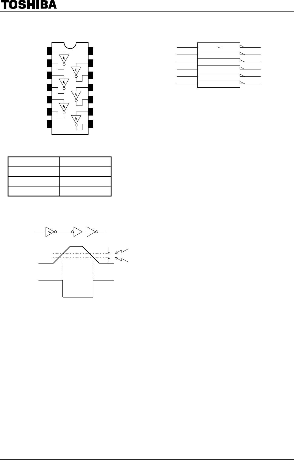
Low-Voltage Hex Schmitt Inverter with 5-V Tolerant Inputs and Outputs
The TC74LCX14 is a high-performance CMOS schmitt inverter.
Designed for use in 3.3-V systems, it achieves high-speed
operation while maintaining the CMOS low power dissipation.
The device is designed for low-voltage (3.3 V) V
CC
applications,
but it could be used to interface to 5-V supply environment for
inputs.
Pin configuration and function are the same as the
TC74LCX04 but the inputs have hysteresis and with Schmitt
trigger function, the TC74LCX14F/FT/FK can be used as line
receivers which will receive slow input signals.
All inputs are equipped with protection circuits against static
discharge.
Features
Low-voltage operation: V
CC
= 1.65 to 3.6 V
High-speed operation: t
pd
= 6.5 ns (max) (V
CC
= 3.0 to 3.6 V)
Ouput current: |I
OH
|/I
OL
= 24 mA (min) (V
CC
= 3.0 V)
Latch-up performance: >±500 mA
Available in JEITA SOP, TSSOP and VSSOP (US)
Power-down protection provided on all inputs and outputs
Pin and function compatible with the 74 series
(74AC/VHC/HC/F/ALS/LS etc.) 14 type
Weight
SOP14-P-300-1.27A : 0.18 g (typ.)
TSSOP14-P-0044-0.65A : 0.06 g (typ.)
VSSOP14-P-0030-0.50 : 0.02 g (typ.)
Note: The Electrical Characteristics of V
CC
=1.8±0.15V is only applicable for products which manufactured
from January 2009 onward.
.
TC74LCX14F
TC74LCX14FT
TC74LCX14FK
Start of commercial production
1995-02
TC74LCX14F/FT/FK
2014-03-01
2
Pin Assignment
(top view)
IEC Logic Symbol
Truth Table
Inputs Outputs
A Y
L H
H L
System Diagram and waveform
1A
2A
3A
4A
5A
6A
1Y
2Y
3Y
4Y
5Y
6Y
(1)
(3)
(5)
(9)
(11)
(13)
(2)
(4)
(6)
(8)
(10)
(12)
V
CC
14
6A
6Y
5A
5Y
4A
13
12
11
10
9
8
1A 1
2
3
4
5
6
7
1Y
2A
2Y
3A
3Y
GND
4Y
V
N
V
H
Y
V
P
A
V
IN
(A)
V
OUT
(Y)
TC74LCX14F/FT/FK
2014-03-01
3
Absolute Maximum Ratings (Note 1)
Characteristics Symbol Rating Unit
Power supply voltage V
CC
0.5 to 7.0 V
DC input voltage V
IN
0.5 to 7.0 V
0.5 to 7.0 (Note 2)
DC output voltage V
OUT
0.5 to V
CC
+ 0.5
(Note 3)
V
Input diode current I
IK
50 mA
Output diode current I
OK
±50 (Note 4) mA
DC output current I
OUT
±50 mA
Power dissipation P
D
180 mW
DC V
CC
/ground current I
CC
/I
GND
±100 mA
Storage temperature T
stg
65 to 150 °C
Note 1: Exceeding any of the absolute maximum ratings, even briefly, lead to deterioration in IC performance or
even destruction.
Using continuously under heavy loads (e.g. the application of high temperature/current/voltage and the
significant change in temperature, etc.) may cause this product to decrease in the reliability significantly
even if the operating conditions (i.e. operating temperature/current/voltage, etc.) are within the absolute
maximum ratings and the operating ranges.
Please design the appropriate reliability upon reviewing the Toshiba Semiconductor Reliability Handbook
(“Handling Precautions”/“Derating Concept and Methods”) and individual reliability data (i.e. reliability test
report and estimated failure rate, etc).
Note 2: V
CC
= 0 V
Note 3: High or low state. I
OUT
absolute maximum rating must be observed.
Note 4: V
OUT
< GND, V
OUT
> V
CC
Operating Ranges (Note 1)
Characteristics Symbol Rating Unit
1.65 to 3.6
Power supply voltage V
CC
1.5 to 3.6 (Note 2)
V
Input voltage V
IN
0 to 5.5 V
0 to 5.5 (Note 3)
Output voltage V
OUT
0 to V
CC
(Note 4)
V
±24 (Note 5)
Output current I
OH
/I
OL
±12 (Note 6)
mA
Operating temperature T
opr
40 to 85 °C
Note 1: The operating ranges must be maintained to ensure the normal operation of the device.
Unused inputs must be tied to either V
CC
or GND.
Note 2: Data retention only
Note 3: V
CC
= 0 V
Note 4: High or low state
Note 5: V
CC
= 3.0 to 3.6 V
Note 6: V
CC
= 2.7 to 3.0 V

TC74LCX14FK(EL,K)

Mfr. #:
Manufacturer:
Toshiba
Description:
Inverters CMOS Logic IC 6.5ns 24mA 1.65 to 3.6V
Lifecycle:
New from this manufacturer.
Delivery:
DHL FedEx Ups TNT EMS
Payment:
T/T Paypal Visa MoneyGram Western Union

Products related to this Datasheet