Expand menu
Hello, Sign in
My Account
0
Cart
Home
Products
Sensors
Semiconductors
Passive Components
Connectors
Power
Electromechanical
Optoelectronics
Circuit Protection
Integrated Circuits - ICs
Main Products
Manufacturers
Blog
Services
About OMO
About Us
Contact Us
Check Stock
CPF0402B20RE
P1-P3
P4-P6
P7-P9
Thin Film Precision Resistors
1773200 CIS
WR 10/2016
Dimensions in
millimetres unless
otherwise specified
Dimensions Shown for
reference purposes only.
Specifications subject to
change
For Email, phone or live chat,
go to: www.te.com/help
Packaging
Packing Quantity and
Reel Specificati
o
n
Size
ØA ±1.0
ØB ±1.0
ØC ±0.7
W ±1.0
T ±1.0
Paper Tape
Embossed Plastic
Tape
0201
178.0
60.0
13.5
9.5
11.5
1000 / 10000
N/A
0402
0603
1000 / 5000
0805
1206
1210
2010
13.5
15.5
N/A
4000
2512
Paper tape Specificati
o
n
Size
A ±0.05
B ±0.05
W
±0.10
E
±0.05
F ±0.05
P
P
P ±.
ØD
T
0201
0.40
0.70
8.00
1.75
3.5
4.00 ±0.10
2.00
±0.05
2.00
1.55 ±0.03
0.42
±0.02
0402
0.70
1.16
1.55 ±0.05
0.40
±0.03
0603
1.10
1.90
4.00
±0.10
0.60
±0.03
0805
1.60
2.37
0.75
±0.05
1206
2.00
3.55
1210
2.75
3.40
4.00 ±0.05
1.60 ±0.10
Thin Film Precision Resistors
1773200 CIS
WR 10/2016
Dimensions in
millimetres unless
otherwise specified
Dimensions Shown for
reference purposes only.
Specifications subject to
change
For Email, phone or live chat,
go to: www.te.com/help
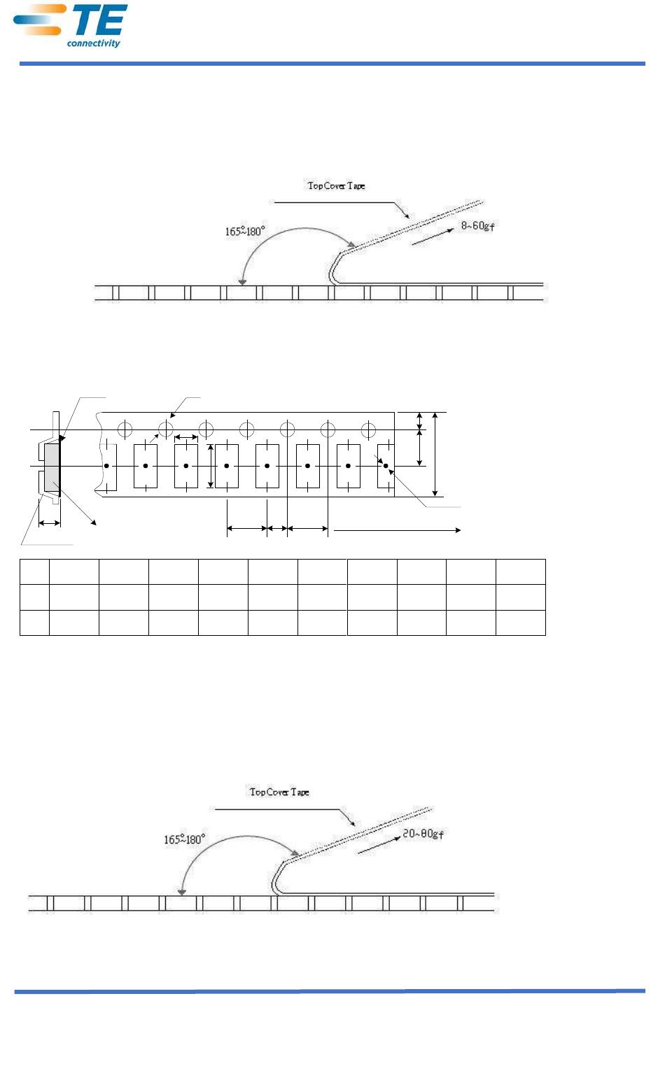
Peel force of top
cover tap
e
The peel spe
ed shall be a
bout 300mm/min±5%
The peel f
orce of top co
ver tape shall be bet
ween 8gf to 60gf
Embossed Plastic Tap
e Specifications
W
E
F
ψ D
0
P
1
P
2
P
0
direction of unreeling
A
B
Top Tape
Resistor
Emboss Tape
T
ψ D
1
1.4Min.
Type
A
B
W
E
F
P
0
P
1
P
2
ØD
0
T
2010
2.85±0.10
5.45±0.10
12.0±0.10
1.75±0.10
5.5±0.05
4.00±0.05
4.00±0.10
2.00±0.05
1.50+0.10
1.00±0.20
2512
3.40±0.10
6.65±0.10
12.0±0.10
1.75±0.10
5.5±0.05
4.00±0.05
4.00±0.10
2.00±0.05
1.50+0.10
1.00±0.20
Peel force of top
cover tap
e
The peel spe
ed shall be a
bout 300mm/min±5%
The peel f
orce of top co
ver tape shall be be
tween 20gf t
o 80g
Thin Film Precision Resistors
1773200 CIS
WR 10/2016
Dimensions in
millimetres unless
otherwise specified
Dimensions Shown for
reference purposes only.
Specifications subject to
change
For Email, phone or live chat,
go to: www.te.com/help
Reel dimension (mm)
Qty / Reel
A ±0.5
B ±0.5
C ±0.5
D ±1
M ±2
W ±1
2000
2
13.5
21
60
178
13.8
Handling Recommendations
When flow soldering -
the land width mus
t be smaller than
the Chip Resistor
width to properly contr
ol the solde
r application. Gene
rally, the land width
can be Chip Resist
or width (W) x 0.
7 to 0.8. When
reflow soldering
–
solder
application amount can be
adjusted. Thus the land wid
th can be set to W
x
1.0 to 1.3.
How To Order
3521
1K0
F
T
Common Part
Resistance Value
Tolerance
Pack Style
1 ohm 1R0
3521
1K ohm 1000 oh
ms
1K0
F
–
1%
J
–
5%
T
–
2000
reel
1 Meg ohm
1000000 ohms
1M0
Reflow Solder Profile
Time of Reflow solder
ing at max
imum temperature point
260°C = 10s
Wave Solder Profile
Time of Wave so
ldering at maximum te
mperature point 26
0°C = 10s
Time of Soldering Iron
at maximum te
mperature point 410°C = 5s
How To Order
CPF
0603
B
100R
E
1
Common Part
Package Size
Tolerance
Value
TCR
Packaging
CPF
- prec
ision
thin film chip
resistor
0201
0402
0603
0805
1206
1210
2010
2512
B
- ±0.1%
D
- ±0.5%
F
- ±1%
100R -
Ω
1K0 -
Ω
10K
–
,Ω
D
–
15PPM
E -
25PPM
C -
50PPM
1
–
1K REEL
Blank
–
standard reel
0201 0402 - 10K
0603 0805 1206 1210
–
5K
2010 2512 -
4K
P1-P3
P4-P6
P7-P9
CPF0402B20RE
Mfr. #:
Buy CPF0402B20RE
Manufacturer:
Description:
Thin Film Resistors - SMD CPF 0402 20R 0.1% 25PPM 5K RL
Lifecycle:
New from this manufacturer.
Delivery:
DHL
FedEx
Ups
TNT
EMS
Payment:
T/T
Paypal
Visa
MoneyGram
Western
Union
Products related to this Datasheet
CPF0603B820KE
CPF0402F100RE1
CPF1206B11R8E1
CPF0603B115RE1
CPF0402B2K87E1
CPF0805B768KE
CPF0402F20KE1
CPF1206B9K76E1
CPF0402B9K53E1
CPF0805B8K2E
CPF0603F681RC1
CPF0402B71R5E1
CPF0402B910RE1
CPF0603F976RC1
CPF0402B53R6E1
CPF0805B2K49E1
CPF0805B71K5E1
CPF0603F1K24C1
CPF0402F53K6E1
CPF0603B130RE1
CPF1206B4K12E1
CPF0805B73R2E1
CPF0603B402KE1
CPF0805B6K81E1
CPF1206B562RE1
CPF0603F59RC1
CPF0805B6R49E1
CPF0603F42K2C1
CPF0603F5K36C1
CPF1206B1K21E1
CPF0603F7K5C1
CPF1206B12K1E1
CPF0402B3K65E1
CPF0402B48R7E1
CPF0805B2K1E1
CPF0603F8K66C1