28
COMMERCIAL AND INDUSTRIAL
TEMPERATURE RANGES
IDT72V3640/50/60/70/80/90 3.3V HIGH DENSITY SUPERSYNC II
TM
36-BIT FIFO
1,024 x 36, 2,048 x 36, 4,096 x 36, 8,192 x 36, 16,384 x 36 and 32,768 x 36
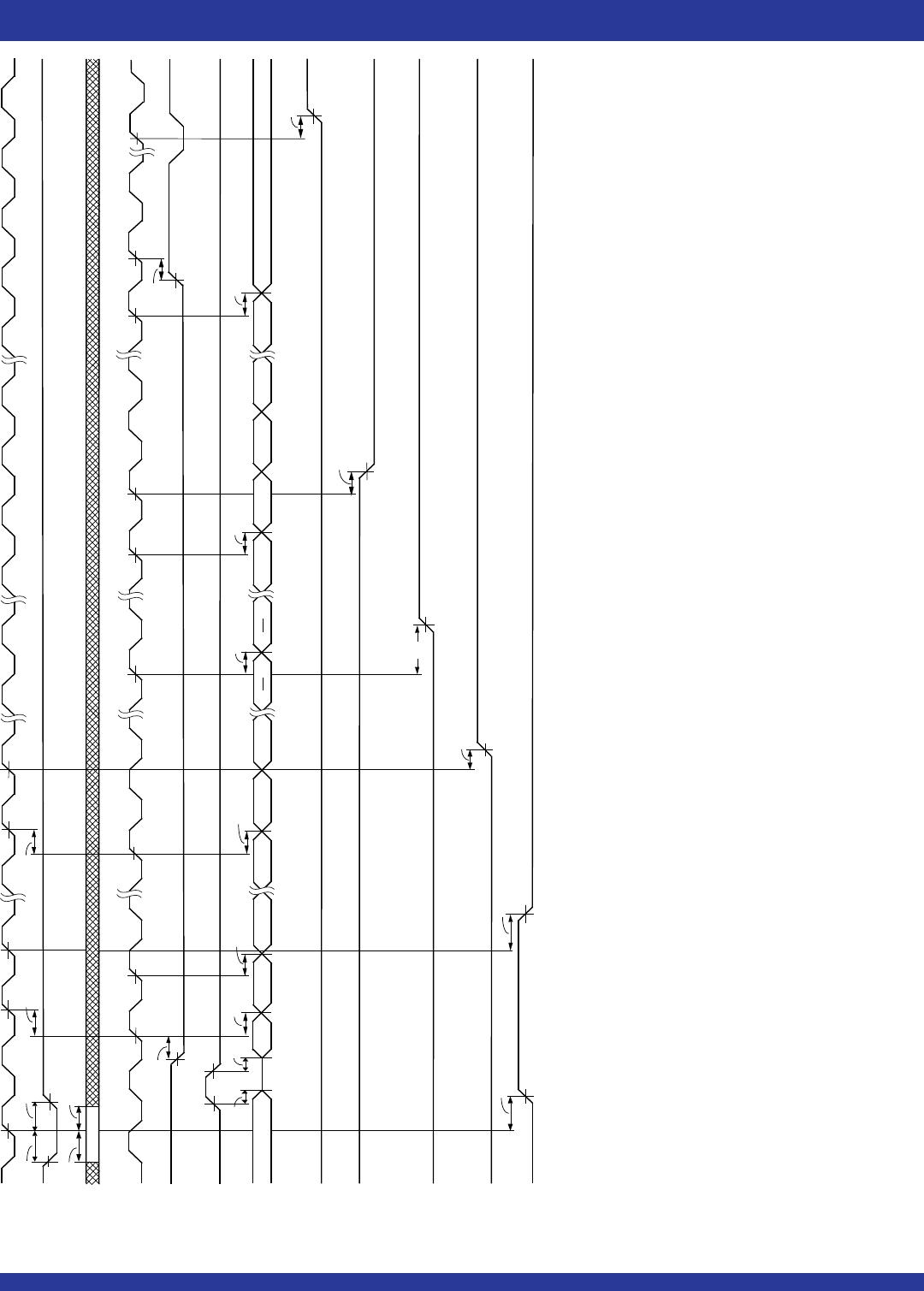
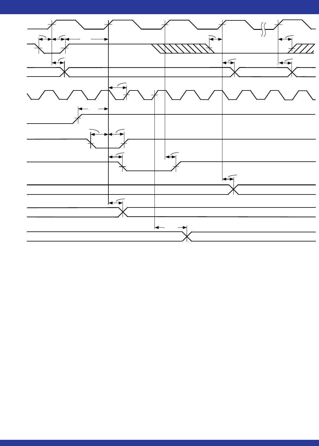
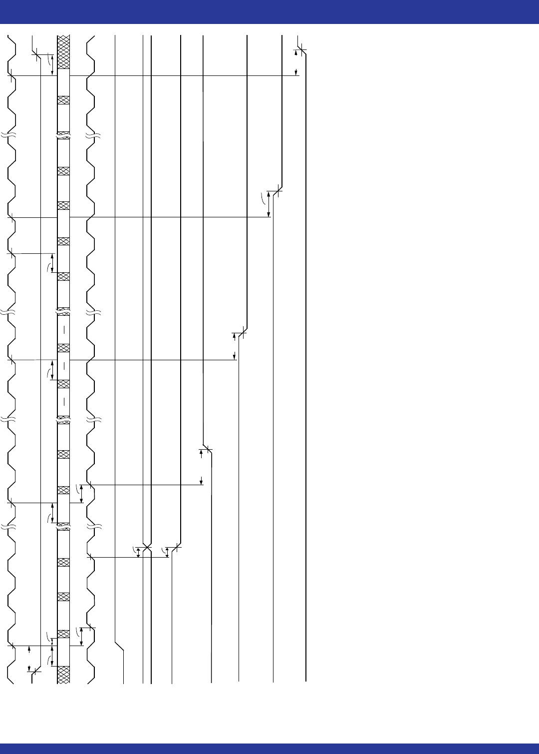
Figure 9. Write Timing (First Word Fall Through Mode)
NOTES:
1. t
SKEW1 is the minimum time between a rising WCLK edge and a rising RCLK edge to guarantee that OR will go LOW after two RCLK cycles plus tREF. If the time between the rising edge of WCLK and the rising edge of RCLK is less than
t
SKEW1, then OR assertion may be delayed one extra RCLK cycle.
2. t
SKEW2 is the minimum time between a rising WCLK edge and a rising RCLK edge to guarantee that PAE will go HIGH after one RCLK cycle plus tPAES. If the time between the rising edge of WCLK and the rising edge of RCLK is less than
t
SKEW2, then the PAE deassertion may be delayed one extra RCLK cycle.
3. LD = HIGH, OE = LOW
4. n = PAE offset, m = PAF offset and D = maximum FIFO depth.
5. D = 1,025 for IDT72V3640, 2,049 for IDT72V3650, 4,097 for IDT72V3660, 8,193 for IDT72V3670, 16,385 for the IDT72V3680 and 32,769 for the IDT72V3690.
6. First data word latency = t
SKEW1 + 2*TRCLK + tREF.
W
1
W
2
W
4
W
[n +2]
W
[D-m-1]
W
[D-m-2]
W
[D-1]
W
D
W
[n+3]
W
[n+4]
W
[D-m]
W
[D-m+1]
WCLK
WEN
D
0
- D
17
RCLK
t
DH
t
DS
t
SKEW1
(1)
REN
Q
0
- Q
17
PAF
HF
PAE
IR
t
DS
t
DS
t
DS
t
SKEW2
t
A
t
REF
OR
t
PAES
t
HF
t
PAFS
t
WFF
W
[D-m+2]
W
1
t
ENH
4667 drw14
DATA IN OUTPUT REGISTER
(2)
W
3
1
2
3
1
D-1
2
+1
][
W
D-1
+2
][
W
2
D-1
+3
][
W
2
1
2
t
ENS