REV. 0
Information furnished by Analog Devices is believed to be accurate and
reliable. However, no responsibility is assumed by Analog Devices for its
use, nor for any infringements of patents or other rights of third parties
which may result from its use. No license is granted by implication or
otherwise under any patent or patent rights of Analog Devices.
a
AD5203
One Technology Way, P.O. Box 9106, Norwood, MA 02062-9106, U.S.A.
Tel: 781/329-4700 World Wide Web Site: http://www.analog.com
Fax: 781/326-8703 © Analog Devices, Inc., 1998
4-Channel, 64-Position
Digital Potentiometer
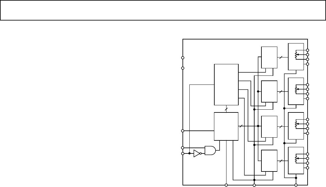
FUNCTIONAL BLOCK DIAGRAM
SHDN
DAC 1
A1
W1
B1
AGND1
6
V
DD
DGND
SDI
CLK
CS
AD5203
SDO
SHDN
A2
W2
B2
AGND2
A3
W3
B3
AGND3
A4
W4
B4
AGND4
6
2
RS
6-BIT
LATCH
CK
RS
6
6-BIT
LATCH
CK
RS
SHDN
DAC 2
SHDN
DAC 3
6
6
SHDN
DAC 4
6-BIT
LATCH
CK
RS
6-BIT
LATCH
CK
RS
DAC
SELECT
A1, A0
1
2
3
4
8-BIT
SERIAL
LATCH
D
CK
Q
RS
FEATURES
64 Position
Replaces Four Potentiometers
10 k, 100 k
Power Shutdown—Less than 5 A
3-Wire SPI-Compatible Serial Data Input
10 MHz Update Data Loading Rate
+2.7 V to +5.5 V Single Supply Operation
Midscale Preset
APPLICATIONS
Mechanical Potentiometer Replacement
Programmable Filters, Delays, Time Constants
Volume Control, Panning
Line Impedance Matching
Power Supply Adjustment
GENERAL DESCRIPTION
The AD5203 provides a quad channel, 64-position digitally-
controlled variable resistor (VR) device. These parts perform the
same electronic adjustment function as a potentiometer or vari-
able resistor. The AD5203 contains four independent variable
resistors in a 24-lead SOIC and the compact TSSOP-24 pack-
ages. Each part contains a fixed resistor with a wiper contact
that taps the fixed resistor value at a point determined by a digi-
tal code loaded into the controlling serial input register. The
resistance between the wiper and either endpoint of the fixed
resistor varies linearly with respect to the digital code transferred
into the VR latch. Each variable resistor offers a completely
programmable value of resistance, between the A terminal and
the wiper or the B terminal and the wiper. The fixed A-to-B
terminal resistance of 10 k, or 100 k has a ±1% channel-to-
channel matching tolerance with a nominal temperature coeffi-
cient of 700 ppm/°C.
Each VR has its own VR latch which holds its programmed
resistance value. These VR latches are updated from an internal
serial-to-parallel shift register that is loaded from a standard
3-wire serial-input digital interface. Eight data bits make up the
data word clocked into the serial input register. The data word is
decoded where the first two bits determine the address of the VR
latch to be loaded, the last 6-bits are data. A serial data output
pin at the opposite end of the serial register allows simple daisy-
chaining in multiple VR applications without additional external
decoding logic.
The reset RS pin forces the wiper to the midscale position by
loading 20
H
into the VR latch. The SHDN pin forces the resis-
tor to an end-to-end open circuit condition on terminal A and
shorts the wiper to terminal B, achieving a microwatt power
shutdown state. When shutdown is returned to logic-high the
previous latch settings put the wiper in the same resistance set-
ting prior to shutdown.
The AD5203 is available in a narrow body P-DIP-24, the
24-lead surface mount package, and the compact 1.1 mm thin
TSSOP-24 package. All parts are guaranteed to operate over the
extended industrial temperature range of –40°C to +85°C.
For pin compatible higher resolution applications, see the 256-
position AD8403 product.
AD5203* PRODUCT PAGE QUICK LINKS
Last Content Update: 02/23/2017
COMPARABLE PARTS
View a parametric search of comparable parts.
DOCUMENTATION
Application Notes
AN-1291: Digital Potentiometers: Frequently Asked
Questions
AN-580: Programmable Oscillator Uses Digital
Potentiometers
AN-582: Resolution Enhancements of Digital
Potentiometers with Multiple Devices
AN-686: Implementing an I
2
C
®
Reset
Data Sheet
AD5203: 4-Channel, 64-Position Digital Potentiometer
Data Sheet
SOFTWARE AND SYSTEMS REQUIREMENTS
Digital Potentiometer Linux Driver
DESIGN RESOURCES
AD5203 Material Declaration
PCN-PDN Information
Quality And Reliability
Symbols and Footprints
DISCUSSIONS
View all AD5203 EngineerZone Discussions.
SAMPLE AND BUY
Visit the product page to see pricing options.
TECHNICAL SUPPORT
Submit a technical question or find your regional support
number.
DOCUMENT FEEDBACK
Submit feedback for this data sheet.
This page is dynamically generated by Analog Devices, Inc., and inserted into this data sheet. A dynamic change to the content on this page will not
trigger a change to either the revision number or the content of the product data sheet. This dynamic page may be frequently modified.
–2 REV. 0
AD5203–SPECIFICATIONS
ELECTRICAL CHARACTERISTICS
Parameter Symbol Conditions Min Typ
1
Max Units
DC CHARACTERISTICS RHEOSTAT MODE Specifications Apply to All VRs
Resistor Differential NL
2
R-DNL R
WB
, V
A
= No Connect –0.25 ±0.1 +0.25 LSB
Resistor Nonlinearity Error
2
R-INL R
WB
, V
A
= No Connect –0.5 ±0.1 +0.5 LSB
Nominal Resistor Tolerance
3
R
AB
–30 +30 %
Resistance Temperature Coefficient R
AB
/TV
AB
= V
DD
, Wiper = No Connect 700 ppm/°C
Wiper Resistance R
W
I
W
= 1 V/R
AB
45 100
Nominal Resistance Match R/R
O
CH 1 to CH 2,
V
AB
= V
DD
, T
A
= +25°C 0.2 1 %
DC CHARACTERISTICS POTENTIOMETER DIVIDER MODE Specifications Apply to All VRs
Resolution N 6 Bits
Differential Nonlinearity Error
4
DNL –0.25 ±0.1 +0.25 LSB
Integral Nonlinearity Error
4
INL –0.75 ±0.1 +0.75 LSB
Voltage Divider Temperature Coefficient V
W
/T Code = 20
H
20 ppm/°C
Full-Scale Error V
WFSE
Code = 3F
H
–0.75 –0.2 0 LSB
Zero-Scale Error V
WZSE
Code = 00
H
0 +0.1 +0.75 LSB
RESISTOR TERMINALS
Voltage Range
5
V
A,
V
B,
V
W
0V
DD
V
Capacitance
6
Ax, Bx C
A,
C
B
f = 1 MHz, Measured to GND, Code = 20
H
75 pF
Capacitance
6
Wx C
W
f = 1 MHz, Measured to GND, Code = 20
H
120 pF
Shutdown Supply Current
7
I
A_SD
V
A
= V
DD
, V
B
= 0 V, SHDN = 0 0.01 5 µA
Shutdown Wiper Resistance R
W_SD
V
A
= V
DD
, V
B
= 0 V, SHDN = 0, V
DD
= +5 V 45 100
DIGITAL INPUTS AND OUTPUTS
Input Logic High V
IH
V
DD
= +5 V 2.4 V
Input Logic Low V
IL
V
DD
= +5 V 0.8 V
Input Logic High V
IH
V
DD
= +3 V 2.1 V
Input Logic Low V
IL
V
DD
= +3 V 0.6 V
Output Logic High V
OH
R
L
= 2.2 k to V
DD
V
DD
–0.1 V
Output Logic Low V
OL
I
OL
= 1.6 mA, V
DD
= +5 V 0.4 V
Input Current I
IL
V
IN
= 0 V or +5 V, V
DD
= +5 V ±1 µA
Input Capacitance
6
C
IL
5pF
POWER SUPPLIES
Power Supply Range V
DD
Range 2.7 5.5 V
Supply Current (CMOS) I
DD
V
IH
= V
DD
or V
IL
= 0 V 0.01 5 µA
Supply Current (TTL)
8
I
DD
V
IH
= 2.4 V or V
IL
= 0.8 V, V
DD
= +5.5 V 0.9 4 mA
Power Dissipation (CMOS)
9
P
DISS
V
IH
= V
DD
or V
IL
= 0 V, V
DD
= +5.5 V 27.5 µW
Power Supply Sensitivity PSS V
DD
= +5 V ± 10% 0.0002 0.001 %/%
PSS V
DD
= +3 V ± 10% 0.006 0.03 %/%
DYNAMIC CHARACTERISTICS
6, 10
Bandwidth –3 dB BW_10K R
AB
= 10 k 600 kHz
BW_100K R
AB
= 100 k 71 kHz
Total Harmonic Distortion THD
W
V
A
=1 V rms + 2 V dc, V
B
= 2 V dc, f = 1 kHz 0.003 %
V
W
Settling Time t
S
_10K V
A
= V
DD
, V
B
= 0 V, ±1 LSB Error Band 2 µs
t
S
_100K V
A
= V
DD
, V
B
= 0 V, ±1 LSB Error Band 18 µs
Resistor Noise Voltage e
NWB
R
WB
= 5 k, f = 1 kHz, RS = 0 9 nV/Hz
R
WB
= 50 k, f = 1 kHz, RS = 0 29 nV/Hz
Crosstalk
11
C
T
V
A
= V
DD
, V
B
= 0 V –65 dB
INTERFACE TIMING CHARACTERISTICS Applies to All Parts
6, 12
Input Clock Pulsewidth t
CH
, t
CL
Clock Level High or Low 10 ns
Data Setup Time t
DS
5ns
Data Hold Time t
DH
5ns
CLK to SDO Propagation Delay
13
t
PD
R
L
= 2.2 k, C
L
< 20 pF 1 25 ns
CS Setup Time t
CSS
10 ns
CS High Pulsewidth t
CSW
10 ns
Reset Pulsewidth t
RS
50 ns
CLK Fall to CS Rise Hold Time t
CSH
0ns
CS Rise to Clock Rise Setup t
CS1
10 ns
(V
DD
= +3 V 10% or +5 V 10%, V
A
= +V
DD
, V
B
= 0 V, –40C < T
A
< +85C unless
otherwise noted)

AD5203ARUZ100

Mfr. #:
Manufacturer:
Analog Devices Inc.
Description:
Digital Potentiometer ICs QUAD 6-Bit POTENTIOMETER
Lifecycle:
New from this manufacturer.
Delivery:
DHL FedEx Ups TNT EMS
Payment:
T/T Paypal Visa MoneyGram Western Union